Organic Field-Effect Transistors for Vapor-Phase Explosive Detection: Mechanisms, Materials, and Future Frontiers
This article provides a comprehensive review of Organic Field-Effect Transistors (OFETs) as next-generation sensors for detecting vapor-phase explosives.
Organic Field-Effect Transistors for Vapor-Phase Explosive Detection: Mechanisms, Materials, and Future Frontiers
Abstract
This article provides a comprehensive review of Organic Field-Effect Transistors (OFETs) as next-generation sensors for detecting vapor-phase explosives. Tailored for researchers and scientists in material science and security diagnostics, it explores the foundational principles of OFET-based sensing, detailing how molecular engineering of organic semiconductors enhances sensitivity and selectivity. The scope covers advanced fabrication methodologies, critical performance optimization strategies to overcome operational instability, and a comparative analysis with established technologies like canine units and SERS. By synthesizing recent progress (2018-2024) with future outlooks, this article serves as a strategic guide for developing high-performance, flexible, and low-cost explosive detection systems.
The Foundation of OFET Sensing: Principles and Material Design for Explosive Vapors
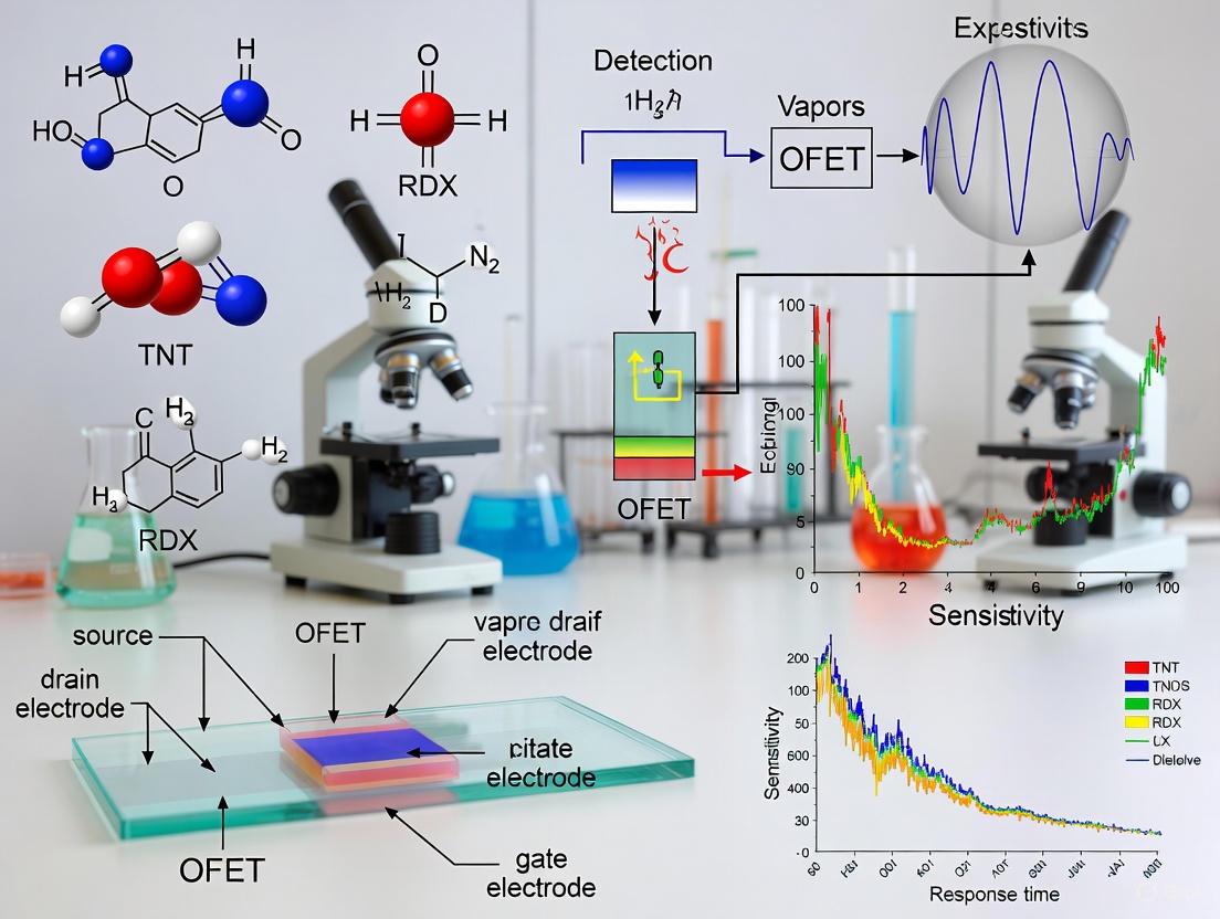
Organic Field-Effect Transistors (OFETs) are solid-state devices that use an organic semiconductor layer to modulate current flow between source and drain terminals via an applied gate voltage. As an alternative to silicon-based transistors, OFETs form the foundational building block for a new generation of sensors, particularly for vapor phase explosive detection, owing to their unique combination of mechanical flexibility, low-cost fabrication, and superior sensing capabilities at the organic semiconductor-analyte interface [1] [2]. Their operation as amplification devices enables the detection of very weak signals, making them exceptionally suitable for identifying low-concentration analytes in complex mixtures [3].
Core Components and Architecture
A typical OFET consists of five fundamental components, each playing a critical role in device operation and sensing performance [1] [2].
- Electrodes (Source, Drain, and Gate): The source and drain electrodes facilitate the injection and extraction of charge carriers (holes or electrons) into the organic semiconductor layer. The gate electrode acts as the primary control terminal, applying an electric field that modulates the conductivity of the semiconductor channel [1]. Materials like gold, silver, or carbon-based inks are commonly used, often applied via inkjet printing for compatibility with flexible substrates [2] [4].
- Organic Semiconductor (OSC) Layer: This is the active layer where charge transport occurs and the primary site for interaction with target analytes. Charge transport happens through hopping between localized states in conjugated π-molecular frameworks [1]. The chemical structure of the OSC—whether small molecules like TIPS-pentacene or polymers like P3HT—determines key properties such as charge carrier mobility and environmental stability [2] [4].
- Dielectric Layer: This insulating layer separates the gate electrode from the semiconductor layer. When a voltage is applied to the gate, charge carriers accumulate at the semiconductor-dielectric interface, forming the conduction channel [1]. The dielectric's properties (e.g., capacitance, polarity) significantly impact operational voltage and stability. Low-k, non-polar polymers like poly(vinyl cinnamate) can enhance air stability by reducing water adsorption [4].
- Substrate: The physical support for the entire device. For flexible sensors, substrates include plastics like polyethylene naphthalate (PEN), polyethylene terephthalate (PET), or polyimide (PI) [2].
OFETs are primarily categorized by the spatial arrangement of their components, leading to four common architectures [1] [2]:
- Bottom-Gate, Bottom-Contact (BGBC): The gate and source/drain electrodes are on the substrate, with the OSC layer deposited on top. This architecture is experimentally accessible but leaves the semiconductor exposed [1].
- Bottom-Gate, Top-Contact (BGTC): The gate is on the substrate, but the source/drain electrodes are deposited on top of the OSC layer, leading to lower contact resistance [2].
- Top-Gate, Bottom-Contact (TGBC): The source/drain electrodes and OSC are on the substrate, with the dielectric and gate deposited on top. This offers better stability as the organic layer is buried [1].
- Top-Gate, Top-Contact (TGTC): The source/drain and OSC are on the substrate, with the dielectric and gate on top, and contacts made through the dielectric. This provides good encapsulation [1].
Table 1: Primary OFET Architectural Configurations and Their Characteristics [1] [2]
| Architecture | Stability | Experimental Accessibility | Contact Resistance | Best Use Cases |
|---|---|---|---|---|
| BGBC | Low (OSC exposed) | High | Moderate | Prototyping, fundamental studies |
| BGTC | Low (OSC exposed) | Moderate | Low | Performance-optimized lab devices |
| TGBC | High (OSC buried) | Moderate | Moderate | Sensors requiring higher stability |
| TGTC | High (OSC buried) | Low | Low | Stable, encapsulated devices |
Operational Principles and Sensing Mechanism
Fundamental OFET Operation
OFET operation relies on the field-effect to control the conductivity of a semiconductor channel. In a p-type OFET, applying a negative gate voltage ((VG)) induces a positive charge (holes) at the semiconductor-dielectric interface [1]. This creates a conductive pathway for current ((I{DS})) to flow between the source and drain when a voltage ((V_{DS})) is applied. The relationship between drain current and terminal voltages is described by two primary operational regions [2]:
- Linear Region ((V{DS} < VG - VT)): The drain current increases linearly with (V{DS}). (I{DS} = \frac{W}{L} \mu Ci (V{GS} - VT) V_{DS})
- Saturation Region ((V{DS} \geq VG - VT)): The channel pinches off near the drain, and the drain current saturates. (I{DS} = \frac{W}{2L} \mu Ci (V{GS} - V_T)^2)
Where (W) and (L) are the channel width and length, (\mu) is the charge carrier mobility, (Ci) is the dielectric capacitance per unit area, and (VT) is the threshold voltage.
Sensing Mechanism for Vapor Detection
When an OFET is exposed to a target analyte, the interaction induces measurable changes in its electrical characteristics. For vapor phase explosive detection, the primary mechanisms include [3] [5]:
- Charge Trapping: Analyte molecules adsorbed onto the OSC act as charge traps, reducing the number of mobile charge carriers. This typically manifests as a decrease in field-effect mobility ((\mu)) and a negative shift in the threshold voltage ((V_T)) [5].
- Doping/De-doping: Electron-withdrawing explosive vapors (e.g., nitroaromatics) can act as p-type dopants for the OSC, increasing hole concentration. This can cause an increase in the off-current or a positive (V_T) shift [3].
- Modification of Intermolecular Coupling: analyte absorption can swell the OSC or disrupt its crystalline order, reducing the π-orbital overlap between molecules and thus impairing charge transport, leading to reduced mobility [3].
These interactions occur predominantly at the semiconductor-dielectric interface where the conductive channel forms, making this region most critical for sensing [3].
Critical Performance Parameters for Sensing
The performance of an OFET-based sensor is quantified by several key electrical parameters, which serve as the transduction signals for analyte detection [1] [3].
Table 2: Key OFET Performance Parameters and Their Role in Sensing [1] [3] [4]
| Parameter | Symbol | Description | Ideal Value for Sensing | Impact of Analyte Binding |
|---|---|---|---|---|
| Charge Carrier Mobility | (\mu) | Measure of how quickly charge carriers move through the OSC. | High (>0.5 cm²/V·s) | Typically decreases due to charge trapping or structural disorder. |
| Threshold Voltage | (V_T) | The minimum gate voltage required to form the conduction channel. | Low and stable | Shifts depending on the doping/de-doping nature of the analyte. |
| On/Off Current Ratio | (I{ON}/I{OFF}) | Ratio of current in the "on" state to the "off" state. | High (>10⁵) | Can decrease if the off-state current increases. |
| Subthreshold Swing | (S) | Sharpness of the transition from off to on state. | Low (<100 mV/decade) | Can degrade, indicating an increase in interface trap states. |
These parameters are extracted from the transistor's transfer curve ((I{DS}) vs. (V{GS}) at constant (V{DS})) and output curve ((I{DS}) vs. (V{DS}) at various (V{GS})) [1]. A sensing event is recorded as a change in one or more of these parameters.
Experimental Protocols for Vapor Sensing
Fabrication of a BGBC OFET Sensor for Vapor Detection
The following protocol outlines the steps for fabricating a low-voltage, all-solution-processed BGBC OFET, optimized for stable vapor sensing in ambient air, adapted from published research [4].
- Substrate Preparation: Begin with a flexible polyethylene naphthalate (PEN) substrate. Clean sequentially in acetone and isopropanol using an ultrasonic bath for 10 minutes each, then dry under a stream of nitrogen.
- Gate Electrode Patterning: Inkjet print a silver nanoparticle ink onto the PEN substrate to form the gate electrode. Anneal at 145°C for 15 minutes in a convection oven to achieve a conductive film.
- Dielectric Layer Deposition: Spin-coat a solution of poly(vinyl cinnamate) (PVC) in an appropriate solvent onto the substrate, fully covering the gate electrode. Optimize spin speed and solution concentration to achieve a uniform thickness of ~300 nm. Cure the film according to manufacturer specifications.
- Source/Drain Electrode Patterning: Inkjet print silver source and drain electrodes onto the PVC dielectric layer, defining a channel length (L) and width (W) appropriate for your design (e.g., L=100 µm, W=1000 µm). Anneal again at 145°C for 15 minutes.
- Organic Semiconductor Deposition:
- Prepare a blended solution of a small molecule semiconductor (e.g., TIPS-pentacene) and an insulating polymer binder (e.g., Polystyrene) in chlorobenzene.
- Place the substrate on an inclined support (≈10° tilt).
- Use a micropipette to drop-cast the semiconductor solution onto the substrate, covering the channel between the source and drain electrodes. The inclined geometry promotes the formation of long, oriented crystalline domains essential for high charge carrier mobility [4].
- Allow the solvent to evaporate slowly under a covered petri dish.
- Annealing and Characterization: Anneal the completed device at 60°C for 30 minutes to remove residual solvent. Before sensing experiments, characterize the baseline electrical performance (transfer and output curves) using a semiconductor parameter analyzer.
Vapor Sensing Measurement Protocol
This protocol describes the electrical characterization and gas exposure procedure to evaluate the sensor's response to explosive vapors [5].
- Electrical Characterization Setup: Mount the OFET in a sealed, temperature-controlled test chamber with electrical feedthroughs. Connect the source, drain, and gate terminals to a source measure unit (SMU) or a parameter analyzer.
- Baseline Acquisition:
- Flow dry, synthetic air (or nitrogen) through the chamber at a constant rate (e.g., 200 sccm) until stable conditions are reached.
- Measure and record the full transfer characteristic ((I{DS}) vs. (V{GS}) at a constant (V{DS}), e.g., -3 V) by sweeping (V{GS}). Extract the baseline values for mobility ((\mu)), threshold voltage ((V_T)), and on/off ratio.
- For continuous monitoring, switch to a pulsed-gate measurement technique. Apply a constant (V{DS}) (e.g., -3 V) and a constant (V{GS}) in the saturation regime, and record the steady-state (I{DS}) as your baseline current ((I0)) [5].
- Analyte Exposure:
- Introduce the target vapor into the carrier gas stream using a mass flow controller. For explosive vapors like 2,4-dinitrotoluene (DNT), this may involve passing the carrier gas over a heated solid sample or using a calibrated vapor generator.
- Maintain a constant total flow rate. Monitor the drain current ((I_{DS})) over time until it stabilizes at a new value ((I)).
- Response Calculation and Recovery:
- The sensor response can be quantified as the relative change in drain current: (Response = \frac{I - I0}{I0} \times 100\%) [5].
- Alternatively, shifts in (VT) or (\mu) extracted from full transfer curves before and after exposure can be used.
- To test recovery, stop the analyte flow and resume the flow of pure carrier air. Monitor the return of (I{DS}) towards its original baseline.
- Data Analysis: Plot the response as a function of analyte concentration to determine the sensor's sensitivity and limit of detection (LOD). For array-based sensing (e-nose), use pattern recognition algorithms like Principal Component Analysis (PCA) to discriminate between different analytes [5].
The Scientist's Toolkit: Research Reagents and Materials
Table 3: Essential Materials for OFET Sensor Fabrication [2] [5] [4]
| Material Category | Example Materials | Function/Purpose | Key Considerations |
|---|---|---|---|
| Small Molecule OSCs | TIPS-Pentacene, DNTT, Rubrene | Form the high-mobility active channel where sensing occurs. | High purity; crystalline order impacts mobility and stability. |
| Polymer OSCs | P3HT, PBBPyBT | Provide mechanical flexibility and solution processability. | Molecular weight, regioregularity, and side chains affect performance. |
| Dielectric Materials | PVCi, PMMA, PVA | Insulate the gate and define the capacitance. | Low-k, non-polar polymers enhance air stability [4]. |
| Substrates | PEN, PET, PI | Provide mechanical support. | Glass transition temperature, surface energy, and flexibility. |
| Electrode Inks | Silver Nanoparticle Ink, PEDOT:PSS | Form source, drain, and gate contacts. | Conductivity, printability, and work function for charge injection. |
| Receptor Layers | Metalloporphyrins (e.g., Zn-TPP, Cu-TPP) | Enhance selectivity when deposited on the OSC. | Specific interaction with target analytes; morphology is critical [5]. |
Organic Field-Effect Transistors (OFETs) have emerged as a promising platform for the detection of explosive vapors, combining the advantages of organic electronics—such as flexibility, low-cost fabrication, and tunable chemical properties—with the intrinsic signal amplification capability of a transistor [3]. The sensing mechanism in OFETs is governed by the interaction between vapor-phase explosive molecules and the organic semiconductor (OSC) layer, which modulates the electrical characteristics of the device. This application note details the underlying mechanisms, quantitative sensor responses, and standardized experimental protocols for exploiting OFETs in explosive detection, providing a framework for researchers and development professionals engaged in security and sensing technologies.
When explosive vapor molecules interact with the OSC layer, they act as electron donors or acceptors, thereby modulating the charge carrier density and mobility within the conduction channel [3] [6]. This interaction occurs primarily at the OSC/dielectric interface, where the majority of charge transport takes place, leading to measurable changes in key electrical parameters such as the source-drain current ((I{DS})), threshold voltage ((VT)), and field-effect mobility ((\mu)) [3]. The unique current amplification function of transistors enables the detection of exceptionally weak signals, making OFETs highly suitable for sensing trace-level explosives with low vapor pressure, such as 2,4,6-trinitrotoluene (TNT) and Research Department eXplosive (RDX) [7] [8].
Core Sensing Mechanisms
The detection of explosive vapors by OFETs is primarily governed by physicochemical interactions at the semiconductor interface. The following mechanisms are central to sensor response:
Charge Transfer Doping
Explosive analytes often contain nitro-functional groups (-NO₂) which are strongly electron-withdrawing. Upon adsorption onto the OSC surface, these molecules can act as electron acceptors, extracting electrons from a p-type semiconductor (or donating electrons to an n-type semiconductor) [3] [8]. This charge transfer effectively dopes the OSC channel, altering the concentration of free charge carriers (holes or electrons). For instance, the interaction of TNT with a p-type polymer like poly(3-hexylthiophene) (P3HT) leads to a decrease in hole density, manifesting as a reduction in (I_{DS}) [8].
Electrostatic Gating Effect
Adsorbed explosive molecules can influence channel conductivity without direct charge exchange by inducing a localized electric field. This field-effect doping occurs when the analyte's permanent dipole moment or its induced polarization shifts the local potential at the OSC/dielectric interface, effectively acting as a secondary gate [3]. This mechanism can cause significant shifts in the threshold voltage ((V_T)) of the transistor, as the gate voltage required to turn on the device changes to compensate for the additional field.
Morphological and Interfacial Trapping
The infiltration of analyte molecules into the OSC film can disrupt the molecular packing and π-orbital overlapping between adjacent polymer chains [3]. This disruption increases scattering sites and creates charge carrier traps at grain boundaries or intermolecular sites, thereby reducing the effective field-effect mobility ((\mu)) of the semiconductor [3]. In devices based on nanowire (NW) networks, the adsorption of analytes at the NW-NW junctions can modulate the contact resistance between individual nanowires, presenting a dominant resistance in the conduction pathway [7].
The diagram below illustrates the primary sensing mechanisms in an OFET exposed to explosive vapor.
Quantitative Sensor Response Data
The response of an OFET to an explosive vapor is quantified by changes in its electrical parameters. The following table summarizes characteristic responses reported for various explosive analytes and OSC materials.
Table 1: Characteristic OFET Responses to Explosive Vapors
| Explosive Analyte | Organic Semiconductor Material | Key Parameter Change | Reported Magnitude of Change | References |
|---|---|---|---|---|
| TNT (2,4,6-trinitrotoluene) | P3HT/SXFA/CuTPP composite | Drain Current ((I_{DS})) | Significant change in output characteristics enabling classification | [8] |
| RDX | P3HT/SXFA/CuTPP composite | Drain Current ((I_{DS})) | Significant change in output characteristics enabling classification | [8] |
| TNT | Ge Nanowire (NW) Networks | Electrical Resistance | High efficiency post-annealing due to improved NW-NW junction conduction | [7] |
| Nitroaromatics (General) | Functionalized Polymer Composites | Threshold Voltage ((V_T)), Mobility ((\mu)) | Drift dependent on specific analyte-OSC interaction | [3] [8] |
The sensing performance can be further evaluated by calculating the responsivity ((R)). A common metric for chemiresistive-type sensors (a simpler two-terminal configuration related to OFETs) is the relative change in resistance, defined as: [ R = \frac{\Delta R}{R0} = \frac{R{gas} - R0}{R0} ] where (R0) is the baseline resistance in clean air and (R{gas}) is the resistance upon exposure to the target vapor [7]. In a full OFET configuration, the responsivity can also be defined for parameters like (I{DS}) or (I{on}/I_{off}) ratio, with reports exceeding 6500% for some analytes like H₂S, demonstrating the high sensitivity potential of the platform [6].
Experimental Protocols
Protocol: Fabrication of a Bottom-Gate Top-Contact (BGTC) OFET
This protocol outlines the steps for fabricating a common BGTC OFET structure suitable for explosive vapor sensing [8] [2].
Research Reagent Solutions & Essential Materials
Table 2: Key Materials for OFET Fabrication and Sensing
| Item Name | Function / Explanation | Exemplary Materials / Compositions |
|---|---|---|
| Heavily Doped Silicon Wafer | Serves as the substrate and global gate electrode. | (100) orientation with a dry-grown SiO₂ layer (100-300 nm) as the dielectric [8] [2]. |
| Organic Semiconductor (OSC) | Forms the active channel where sensing occurs. | P3HT, PCDTPT, PCDTFBT, or composites like P3HT/SXFA/CuTPP [8] [6]. |
| Source/Drain Electrodes | Provide electrical contact to the OSC layer. | Gold (Au) or other high-work-function metals for p-type OSCs, deposited via thermal evaporation [7] [2]. |
| Surface Treatment | Modifies dielectric surface energy to improve OSC morphology. | Octadecyltrichlorosilane (OTS) [6]. |
| Explosive Vapor Source | Calibrated source of analyte for testing. | Solid TNT or RDX in a sealed vial, often with a vapor generator [8] [9]. |
Procedure:
- Substrate Preparation: Begin with a silicon wafer with a thermally grown oxide layer (SiO₂, ~100-300 nm). Clean the substrate using standard RCA or piranha etch protocols to remove organic contaminants.
- Surface Functionalization (Optional): To control the crystalline morphology of the subsequently deposited OSC, treat the SiO₂ surface with a self-assembled monolayer (e.g., OTS) [6].
- OSC Layer Deposition:
- For polymer OSCs (e.g., P3HT, PCDTPT): Prepare a solution (e.g., 2.5 mg/mL in chloroform or toluene). Spin-coat the solution onto the substrate at a specified speed (e.g., 2000-3000 rpm for 30-60 s). Anneal the film on a hotplate (e.g., 80°C for 10-30 min) to remove residual solvent [6].
- For composite films: Mix the OSC with sensory polymers (e.g., SXFA) or porphyrins (e.g., CuTPP) in solution prior to spin-coating [8].
- Electrode Deposition: Using a shadow mask or photolithography, define the source and drain electrode patterns. Thermally evaporate gold (e.g., 50-100 nm thickness) to form the electrodes [7] [2].
- Post-Processing Anneal (Optional): Some devices may require annealing in an inert or reducing atmosphere (e.g., H₂ at 450°C for 30 min for Ge NWs) to improve crystallinity or remove native oxide, thereby enhancing inter-crystallite conductivity [7].
Protocol: Vapor Sensing Measurement and Data Acquisition
This protocol describes a standard setup and procedure for evaluating the sensing performance of the fabricated OFET.
Apparatus:
- A sealed test chamber equipped with electrical feedthroughs for connecting the OFET to a source/measurement unit (e.g., Keithley 2635B) [7].
- A vapor delivery system consisting of a reservoir (e.g., a 10 mL vial containing solid explosive), mass flow controllers, and tubing [7] [8].
- A data acquisition system to record electrical parameters in real-time.
Procedure:
- Baseline Establishment: Place the OFET inside the test chamber. Flush the chamber with a continuous flow of dry, clean air or inert gas (e.g., N₂). Measure and record the stable baseline transfer characteristics ((I{DS}) vs. (V{GS}) at constant (V{DS})) and/or output characteristics ((I{DS}) vs. (V{DS}) at various (V{GS})) [7] [6].
- Vapor Exposure: Introduce the explosive vapor into the carrier gas stream. This can be done by diverting the carrier flow through a vial containing the solid explosive, typically maintained at a constant temperature to stabilize vapor pressure [7] [8]. A calibrated flow rate (e.g., 20 mL/min) is recommended.
- Response Monitoring: Continuously monitor the change in the chosen electrical parameter(s) over time. Common parameters include (I{DS}) at a fixed (V{GS}) and (V_{DS}), or the entire transfer curve at regular intervals [6].
- Recovery Phase: Stop the vapor flow and revert to the pure carrier gas flow to purge the chamber and desorb the analyte from the OSC surface. Monitor the signal until it returns to the baseline or a new steady state.
The workflow for the sensing measurement is outlined below.
Advanced Applications and Data Analysis
Integration with Artificial Intelligence
The multi-parameter output of OFETs (changes in (I{DS}), (VT), (\mu), etc.) provides a rich dataset for pattern recognition. Machine learning algorithms can be employed to enhance selectivity and quantify analyte concentration [8] [6]. For instance, algorithms such as Naive Bayes Classifier (NBS), Sequential Minimal Optimization (SMO), and J48 decision tree have been used to classify different explosives like RDX and TNT with high accuracy based on multiparametric OFET data [8]. Furthermore, Artificial Neural Networks (ANN) have demonstrated the ability to predict the concentration of a target gas with an error of less than 5% by using multiple independent OFET parameters as input features [6].
Material Engineering for Enhanced Selectivity
A key strategy for improving sensor performance is the chemical design of the OSC layer. Blending the primary OSC with selective receptor materials creates a composite sensory layer. For example, incorporating copper(II) tetraphenylporphyrin (CuTPP) into a P3HT matrix provides specific binding sites for nitroaromatic explosives, leading to improved selectivity [8]. Similarly, using functional polymers like hexafluoro-2-propanol-substituted polysiloxane (SXFA) can tailor the surface interactions to favor the target analyte over potential interferents.
Molecular Engineering of Organic Semiconductors for Targeted Analyte Interaction
Organic Field-Effect Transistors (OFETs) have emerged as a transformative technology for the detection of vapor-phase explosives, combining high sensitivity with the benefits of mechanical flexibility, low-cost fabrication, and room-temperature operation [3]. The core principle of these sensors rests on the interaction between the organic semiconductor (OSC) layer and the target analyte, a process that can be meticulously engineered at the molecular level [3]. This document provides detailed application notes and experimental protocols for the molecular engineering of OSCs to enhance their selectivity and sensitivity towards specific explosive vapors, such as 2,4-dinitrotoluene (2,4-DNT) and related taggants, within the context of OFET-based sensing platforms [10] [11]. We summarize key quantitative data, outline definitive experimental methodologies, and provide essential resources to advance research in this critical field.
Molecular Design Strategies for Targeted Analyte Interaction
The sensing performance of an OFET is fundamentally governed by the chemical structure and solid-state morphology of the organic semiconductor layer. Strategic molecular design is paramount for fostering specific and effective interactions with target explosive analytes. The table below summarizes core molecular engineering strategies and their impact on sensing performance.
Table 1: Molecular Engineering Strategies for Enhanced Analyte Interaction
| Strategy | Molecular Approach | Impact on Sensing Parameters | Exemplary Materials |
|---|---|---|---|
| Functional Group Engineering | Introducing electron-rich or electron-deficient moieties to modulate frontier orbital energies [12]. | Enhances selectivity via specific acid-base or dipole-dipole interactions; improves charge transfer efficiency with analytes [3] [12]. | DFP-4T (perfluoroarene-terminated) [12]. |
| π-Conjugation Tuning | Extending the π-conjugated backbone and minimizing intramolecular torsional angles [12]. | Increases charge carrier mobility and promotes stronger π-π stacking with nitroaromatic analytes, boosting sensitivity [3] [12]. | DFH-4T, DFP-4T [12]. |
| Solid-State Morphology Control | Employing post-treatment processes (e.g., Solvent Vapor Annealing) to manipulate grain boundaries and crystallinity [13]. | Creates more adsorption sites and facilitates analyte diffusion to the charge transport channel, lowering the limit of detection [13]. | TIPS-pentacene [13]. |
| Side-Chain Engineering | Attaching specific side chains (e.g., fluorine-containing groups) to influence packing and surface properties [12]. | Improves molecular packing for efficient charge transport; induces hydrophobicity to mitigate interference from ambient moisture [12]. | DFP-4T [12]. |
The following diagram illustrates the logical workflow for the rational design of an organic semiconductor for targeted analyte interaction, from initial molecular design to final performance validation.
Experimental Protocols
Protocol 1: Fabrication of Nanostructured DFP-4T Films via Physical Vapor Deposition (PVD) for Fluorescence Quenching Sensing
This protocol describes the formation of highly nanostructured, SERS-active films of the small molecule DFP-4T, which can also serve as a sensitive layer for the fluorescence-based detection of explosive vapors through a quenching mechanism [12].
3.1.1 Materials and Equipment
- Organic Semiconductor: Purified 5,5‴-diperfluorophenyl-2,2′:5′,2″:5″,2‴-quaterthiophene (DFP-4T) [12].
- Substrate: Si(001) wafer.
- Deposition System: High-vacuum physical vapor deposition (PVD) chamber capable of maintaining ~10⁻⁶ Torr.
- Characterization: Field Emission Scanning Electron Microscopy (FE-SEM), Atomic Force Microscopy (AFM), X-ray Diffractometer (XRD).
3.1.2 Step-by-Step Procedure
- Substrate Preparation: Clean the Si(001) substrate thoroughly using standard solvent sonication (e.g., acetone, isopropanol) and oxygen plasma treatment.
- Material Loading: Place purified DFP-4T solid in a crucible within the PVD evaporation source.
- System Evacuation: Pump down the deposition chamber to a high vacuum of approximately 10⁻⁶ Torr.
- Film Deposition:
- Set the substrate temperature to a low range of 30–40 °C.
- Use a short source-to-substrate distance of 5–7 cm.
- Initiate thermal evaporation with an ultrafast deposition rate of >40 nm s⁻¹.
- Deposit to a target film thickness of 1.1 ± 0.2 µm.
- Post-Process Handling: Carefully vent the chamber and retrieve the substrate with the nanostructured DFP-4T film.
3.1.3 Critical Parameters
- Deposition Rate: A high rate (>40 nm/s) is critical to promote out-of-plane crystal growth and form vertically aligned nanoplates [12].
- Substrate Temperature: Low temperature (30-40 °C) is essential for inducing the desired nanostructured morphology rather than a flat, polycrystalline film [12].
Protocol 2: Solvent Vapor Annealing (SVA) of TIPS-Pentacene OFETs for Enhanced NO₂ Sensing
This protocol outlines a post-treatment process to manipulate the microstructure of a solution-processed OSC film, thereby enhancing the sensitivity of an OFET-based gas sensor [13].
3.2.1 Materials and Equipment
- Organic Semiconductor: TIPS-pentacene solution in 1,2-dichlorobenzene (8 mg/mL).
- Dielectric: Poly(methyl methacrylate) (PMMA) solution in anisole (10 wt.%).
- Substrate: ITO-coated glass.
- Solvents for SVA: Toluene, o-xylene, 1,3,5-trimethylbenzene (TMB).
- Fabrication Equipment: Spin coater, thermal evaporator for gold electrodes.
- SVA Setup: Sealable petri dish.
- Characterization: OFET parameter analyzer, AFM.
3.2.2 Step-by-Step Procedure
- Device Fabrication:
- Spin-coat PMMA dielectric layer onto pre-cleaned ITO/glass substrate at 1500 rpm for 60 s. Bake at 90 °C for 2 hours.
- Spin-coat TIPS-pentacene layer on top of PMMA at 3000 rpm for 60 s.
- Thermally anneal the film at 125 °C for 15 min on a hotplate to remove residual solvent. This is the "pristine" device.
- Solvent Vapor Annealing Process:
- Pour 2 mL of the selected solvent (e.g., toluene) into a clean petri dish.
- Allow the solvent to equilibrate for 10 minutes at room temperature (25 °C) to create a saturated vapor atmosphere.
- Place the substrate with the TIPS-pentacene film inside the petri dish and seal it for 120 seconds.
- Remove the substrate and rebake at 125 °C for 10 minutes to ensure complete removal of residual solvent.
- Electrode Deposition: Thermally evaporate gold source and drain electrodes (40 nm thickness) through a shadow mask to define the channel (e.g., L=100 µm, W=10 mm).
3.2.3 Critical Parameters
- Solvent Selection: The choice of solvent vapor (e.g., toluene) directly controls the re-organization of the OSC molecules, leading to a optimized density of grain boundaries which act as adsorption sites for gas molecules [13].
- Exposure Time: An exposure time of 120 seconds is typical, but this should be optimized for different solvent and OSC combinations to prevent over-dissolution or underwhelming morphological change [13].
Protocol 3: Thermal Control of Fluorescent Polymer Sensors for Reusable Explosive Detection
This protocol describes the use of thermal modulation to enable the desorption of explosive analytes from a fluorescent polymer sensor, making the sensing process reversible and reusable [10].
3.4.1 Materials and Equipment
- Sensing Polymer: Super Yellow (SY) fluorescent polymer.
- Target Analytes: Vapors of 2,4-DNT, DNB, and the taggant DMDNB.
- Instrumentation: Fluorescence spectroscopy setup with a temperature-controlled sample stage.
3.4.2 Step-by-Step Procedure
- Film Preparation: Prepare a thin film of Super Yellow polymer on a suitable substrate via spin-coating or other appropriate methods.
- Fluorescence Quenching Detection:
- Place the film in the path of the excitation light source and measure the baseline photoluminescence (PL) intensity.
- Expose the film to a trace vapor of the target explosive analyte.
- Monitor the decrease in PL intensity (quenching) due to the interaction with the analyte.
- Thermal Desorption and Recovery:
- After quenching saturation, gradually increase the temperature of the sample stage.
- Monitor the PL intensity in real-time until it recovers to its original baseline value.
- Note the specific desorption temperature at which recovery occurs for different analytes.
3.4.3 Critical Parameters
- Desorption Temperature: The temperature required for complete PL recovery is analyte-specific, providing a secondary discrimination mechanism between different explosives [10].
- Thermal Ramping Rate: A controlled ramp rate is necessary to clearly observe the desorption profile and prevent damage to the organic film.
Performance Metrics and Data Analysis
The quantitative evaluation of sensor performance is critical for comparing different material systems and device architectures. The following table consolidates key performance data from the referenced studies.
Table 2: Quantitative Sensing Performance of Selected Organic Semiconductor Systems
| OSC Material | Sensor Type | Target Analyte | Key Performance Metric | Value | Reference |
|---|---|---|---|---|---|
| DFP-4T | SERS Substrate | Methylene Blue (Model) | Enhancement Factor (EF) | >10⁵ | [12] |
| DFP-4T | SERS Substrate | Methylene Blue (Model) | Limit of Detection (LOD) | 10⁻⁹ M | [12] |
| TIPS-pentacene (SVA-treated) | OFET (OTFT) | NO₂ (10 ppm) | Responsivity Enhancement (vs. pristine) | Order of magnitude | [13] |
| TIPS-pentacene (SVA-treated) | OFET (OTFT) | NO₂ | Limit of Detection (LOD) | 148 ppb | [13] |
| Super Yellow (SY) | Fluorescent Sensor | 2,4-DNT, DNB, DMDNB | Key Feature | Reusable via thermal desorption | [10] |
The following workflow diagram maps the sequence of operations for evaluating a complete OFET-based gas sensor, from material synthesis to data interpretation.
The Scientist's Toolkit: Research Reagent Solutions
This section details essential materials and their specific functions in developing OFET-based explosive vapor sensors.
Table 3: Essential Research Reagents and Materials for OFET-Based Explosive Sensing
| Material/Reagent | Function/Application | Key Properties & Notes |
|---|---|---|
| DFP-4T | SERS-active or fluorescent sensing layer for vapor detection [12]. | Fully π-conjugated; electron-deficient perfluorophenyl end groups; forms nanostructured films via PVD with high enhancement factors [12]. |
| TIPS-pentacene | Solution-processable OSC for OFET active channel; sensitive to NO₂ [13]. | High solubility; functionalization with triisopropylsilylethynyl groups; microstructure highly tunable via SVA [13]. |
| Super Yellow (SY) | Fluorescent polymer for irreversible fluorescence quenching-based detection [10]. | Commercial polymer; enables reusable sensing when paired with a thermal desorption protocol for nitroaromatic explosives [10]. |
| Poly(methyl methacrylate) (PMMA) | Gate dielectric layer in bottom-gate OFET structures [13]. | Provides a smooth, insulating interface for the OSC layer; solution-processable [13]. |
| Polystyrene sulfonate (PSSH) | Electrolyte material for Electrolyte-Gated OFETs (EGOFETs) [14]. | Provides mobile ions for electric double layer formation; enables low-voltage operation (<1 V) [14]. |
| Toluene (Solvent Vapor) | Agent for Solvent Vapor Annealing (SVA) post-treatment [13]. | Selectively swells the OSC film (e.g., TIPS-pentacene) to control crystallinity and grain boundary density, enhancing sensor responsivity [13]. |
Organic Field-Effect Transistors (OFETs) have emerged as a promising platform for the detection of vapor-phase explosives, addressing critical security and environmental monitoring needs. Their appeal lies in a combination of high flexibility, low fabrication cost, excellent substrate conformity, and the rich family of functional organic moieties that can be engineered to selectively react with specific analytes [15] [3]. Compared to traditional inorganic sensors or bulky spectroscopic instruments, OFET-based sensors offer the potential for developing simple, low-cost, portable hand-held systems capable of rapid, on-the-spot analysis [8]. The fundamental sensing principle of an OFET rests on the modulation of its electrical characteristics—such as drain current (IDS), threshold voltage (VTh), or charge carrier mobility (μ)—when analyte molecules interact with the organic semiconductor (OSC) layer [16] [3]. For explosive detection, this often involves electron-deficient nitroaromatic compounds (e.g., TNT, RDX) interacting with electron-donating (p-type) organic semiconductors, leading to measurable changes in the device's electrical output [8] [17].
Defining the Key Performance Metrics
The performance of an OFET-based explosive sensor is quantitatively evaluated using four primary metrics. These metrics collectively define the sensor's operational effectiveness, practicality, and reliability in real-world scenarios.
- Sensitivity refers to the magnitude of the sensor's response to a given change in analyte concentration. In OFETs, it is typically expressed as the relative change in a key electrical parameter, most commonly the drain current (ΔIDS/IDS0), upon exposure to the target explosive vapor [16]. A highly sensitive device will produce a significant signal shift even at low analyte concentrations, which is crucial for detecting elusive explosive vapors.
- Selectivity is the sensor's ability to distinguish the target explosive from other interfering vapors or gases that may be present in the environment (e.g., humidity, common solvents, or other pollutants) [3]. This is achieved by tailoring the chemical structure of the OSC or incorporating specific recognition elements that have a preferential interaction with the target molecule [8] [18].
- Limit of Detection (LOD) is the lowest concentration of the analyte that the sensor can reliably distinguish from background noise. It is a critical parameter for determining the sensor's utility in early warning systems, as explosive vapors are often present at trace levels (parts-per-billion or even parts-per-trillion) [15] [3].
- Response Time and Recovery Time are kinetic parameters that define the sensor's speed. The response time (tres) is the time required for the sensor signal to reach a certain percentage (e.g., 90%) of its maximum response upon analyte exposure. The recovery time (trec) is the time needed for the signal to return to its baseline level after the analyte is removed [16] [3]. Rapid response and recovery are essential for real-time monitoring.
Table 1: Key Performance Metrics and Their Definitions in OFET-Based Explosive Sensing.
| Metric | Definition | Typical Expression in OFETs |
|---|---|---|
| Sensitivity | The change in sensor output per unit change in analyte concentration. | ΔIDS / IDS0 ; ΔV_Th ; Δμ [16] |
| Selectivity | The ability to respond to a target analyte in the presence of interferents. | Ratio of response to target vs. response to other gases [3] |
| Limit of Detection (LOD) | The lowest analyte concentration that can be reliably detected. | Extrapolated concentration yielding a signal-to-noise ratio of 3 [16] |
| Response Time (t_res) | Time to reach 90% of maximum signal upon analyte exposure. | Measured in seconds or minutes [3] |
| Recovery Time (t_rec) | Time for the signal to recover to 10% above baseline after analyte removal. | Measured in seconds or minutes [3] |
Quantitative Performance Data from Literature
Research on OFETs for explosive detection has demonstrated significant progress in optimizing these key metrics. Performance is highly dependent on the materials and device architectures used.
Table 2: Reported Performance Metrics for Selected OFET-Based Explosive Sensors.
| Active Layer/Device Strategy | Target Analyte | Sensitivity (ΔIDS/IDS0) | LOD | Response/Recovery Time | Selectivity Demonstrated Against | Ref. |
|---|---|---|---|---|---|---|
| P3HT/SXFA/CuTPP (Composite) | TNT, RDX | Not explicitly quantified (Data used for classification) | Not specified | Not specified | Good selectivity reported among different nitro-based explosives [8] | [8] |
| 6PTTP6 (Ultrathin Film) | Nitroaromatic Explosive Vapors | ~70% change in mobility | 5 ppm | Not specified | Much more sensitive to target vapors than to humidity [17] | [17] |
| General p-type OSC | NO₂ (Model electron-acceptor) | >100% (for high conc.) | Parts-per-billion (ppb) levels | Ranges from seconds to minutes | Compared with NH₃, NO, SO₂, CO₂ [16] | [16] |
Experimental Protocols for Performance Evaluation
A standardized experimental approach is crucial for the accurate and reproducible characterization of OFET sensors.
Protocol: Fabrication of a Typical OFET Sensor
- Substrate Preparation: Begin with a heavily doped silicon wafer acting as a common global gate. Grow a 100 nm thick layer of SiO₂ via dry oxidation to serve as the gate dielectric [8].
- Gate Dielectric Functionalization (Optional): Treat the SiO₂ surface with oxygen plasma or deposit a self-assembled monolayer (e.g., hexamethyldisilazane, HMDS) to modify the interface properties and improve semiconductor growth [16].
- Organic Semiconductor Deposition: Deposit the OSC layer via spin-coating, drop-casting, or thermal evaporation. For composite films (e.g., P3HT blended with CuTpp or SXFA), prepare solutions of the individual components and blend them prior to deposition [8]. For ultrathin films, carefully control the deposition rate and thickness to within a few molecular monolayers (e.g., ~4 nm) [17].
- Source/Drain Electrode Definition: Use photolithography or shadow masks to thermally evaporate gold or aluminum contacts, defining the channel length (L) and width (W). A high W/L ratio is often maintained to enhance the signal [8].
Protocol: Measuring Sensitivity and LOD
- Baseline Measurement: Place the fabricated OFET in a sealed, temperature-controlled testing chamber. Flow an inert carrier gas (e.g., N₂) or dry air to establish a stable baseline for the device's electrical characteristics (IDS-VGS curves) [8] [16].
- Analyte Exposure: Introduce calibrated vapor streams of the target explosive (e.g., TNT, RDX) at varying concentrations (e.g., from low ppm downwards). Vapor generators calibrated by institutions like the Terminal Ballistics Research Laboratory (TBRL) are used for this purpose [8].
- Data Recording: Continuously monitor the drain current (IDS) at constant source-drain (VDS) and gate (VGS) voltages. Record the change in current (ΔIDS) for each concentration.
- Calculation: Calculate sensitivity as (IDS - IDS0)/IDS0 = ΔIDS / IDS0, where IDS0 is the baseline current [16].
- LOD Determination: Plot the sensitivity (or ΔI_DS) against the analyte concentration. The LOD is extrapolated as the concentration that corresponds to a signal-to-noise ratio of 3 [16].
Protocol: Assessing Selectivity
- Interferent Exposure: Following the same procedure as for the target analyte, expose the OFET sensor to a panel of potential interfering gases and vapors. These may include common VOCs (e.g., acetone, toluene), humidity, NH₃, NO, and CO₂ [16].
- Response Comparison: Measure the sensor's response to each interferent at the same concentration as the target explosive or at their environmentally relevant concentrations.
- Analysis: Calculate the ratio of the response to the target analyte versus the response to each interferent. A high ratio indicates good selectivity for the target [3].
Protocol: Determining Response and Recovery Times
- Rapid Cycling: Expose the sensor to a pulse of the target explosive vapor at a fixed concentration, followed by a purging period with the carrier gas.
- High-Frequency Measurement: Record the I_DS transient with a high sampling rate during the exposure and purging phases.
- Time Constant Extraction: The response time (tres) is the time taken for IDS to rise from baseline to 90% of its maximum saturation value upon analyte exposure. The recovery time (trec) is the time taken for IDS to fall from its maximum value to 10% above the baseline upon purging [3].
Signaling Pathways and Sensing Mechanisms
The sensing mechanism in OFETs for electron-deficient explosives like TNT and RDX primarily involves charge transfer and electrostatic interactions at the semiconductor interface.
Diagram 1: OFET Explosive Sensing Mechanism.
For p-type OFETs, the conduction channel is formed by accumulated hole carriers. When electron-withdrawing nitroaromatic molecules from explosives adsorb onto the OSC surface, they act as charge acceptors, withdrawing electrons from the valence band of the p-type semiconductor. This process increases the hole concentration in the channel, leading to a measurable increase in the drain current [16]. This charge transfer interaction is the cornerstone of sensitivity. Furthermore, the strong dipole moment of nitro-groups can create an electrostatic field that acts as a "local gate," modulating the charge carrier density in the channel and contributing to the threshold voltage shift [3]. The overall workflow, from device fabrication to data analysis, is summarized below.
Diagram 2: OFET Sensor Fabrication and Testing Workflow.
The Scientist's Toolkit: Key Research Reagents and Materials
The performance of an OFET-based explosive sensor is directly linked to the materials used in its construction.
Table 3: Essential Materials for OFET-Based Explosive Sensor Research.
| Material Category | Example Compounds | Function in the Device |
|---|---|---|
| p-type Organic Semiconductors | Poly(3-hexylthiophene) (P3HT), 5,5'-Bis(4-hexylphenyl)-2,2'-bithiophene (6PTTP6) | Forms the active channel; donates electrons to explosive vapors, modulating hole current [8] [17]. |
| Polymer Composites & Binders | Hexafluoro-2-propanol-substituted polysiloxane (SXFA), Copolymer of diethynyl-pentiptycene and dibenzyl-ProDOT (ADB) | Enhances selectivity and sensitivity by providing specific binding sites for explosive molecules [8]. |
| Metalloporphyrin Receptors | Copper(II) tetraphenylporphyrin (CuTPP) | Acts as a Lewis acid receptor, coordinating with nitro groups of explosives to improve selectivity [8]. |
| Gate Dielectrics | Silicon Dioxide (SiO₂), Bovine Serum Albumin (BSA) | Insulating layer that enables field-effect modulation; biomaterials like BSA can add biocompatibility [8] [18]. |
| Source/Drain Electrodes | Gold (Au), Aluminum (Al) | Forms ohmic contacts with the organic semiconductor for charge injection [8]. |
Fabrication and Real-World Application: Building and Deploying OFET Explosive Sensors
Organic field-effect transistors (OFETs) have emerged as a promising platform for the detection of vapor-phase explosives, combining the advantages of mechanical flexibility, low-cost fabrication, and high sensitivity to chemical analytes [3] [19] [20]. The operational principle of OFET-based sensors relies on the modulation of electrical characteristics—such as threshold voltage (VT), field-effect mobility (μFET), and source-drain current (IDS)—when the organic semiconductor (OSC) layer interacts with target analyte molecules [3] [6]. This chemical-to-electrical signal transduction makes OFETs particularly attractive for security and environmental monitoring applications where low-cost, portable, and sensitive detection of explosives is required.
Solution-processing techniques like spin-coating and printing are fundamental to realizing the cost advantage of OFETs, as they eliminate the need for expensive, high-vacuum equipment and enable rapid prototyping [21] [22]. These techniques allow for the deposition and patterning of organic semiconductors and other functional layers on flexible substrates such as polyethylene naphthalate (PEN) or polyethylene terephthalate (PET), which is crucial for developing conformable sensor tags [20] [2]. The performance of the resulting OFET sensors is highly dependent on the morphology, molecular order, and interfacial properties of the OSC layer, all of which can be finely tuned through precise control of processing parameters [21] [23].
This application note provides a detailed overview of spin-coating and printing techniques for fabricating OFET-based vapor sensors, with a specific focus on the detection of explosive-related compounds. It includes structured quantitative data, step-by-step experimental protocols, and essential resource guides to assist researchers in developing and optimizing these sensing platforms.
Spin-Coating Techniques for OFET Fabrication
Fundamental Principles and Parameters
Spin-coating is a widely used technique for depositing uniform thin films of organic semiconductors, with thicknesses typically ranging from a few nanometers to a few microns [24]. The process involves four main stages: (1) Deposition: the OSC solution is dispensed onto a substrate; (2) Spin-up: the substrate is rapidly accelerated to a set speed, spreading the fluid via centrifugal force; (3) Spin-off: excess solution is flung from the substrate, and the film thins due to viscous flow; and (4) Evaporation: solvent evaporates, leading to the formation of a solid film [24]. The final film thickness ((hf)) is inversely proportional to the square root of the spin speed ((\omega)), following the relationship (hf \propto \omega^{-1/2}), and is also influenced by solution concentration, viscosity, and solvent evaporation rate [24].
Table 1: Key Spin-Coating Parameters and Their Impact on OFET Film Properties
| Parameter | Typical Range | Impact on Film Properties | Recommended Value for Vapor Sensing |
|---|---|---|---|
| Spin Speed | 500 - 6000 rpm | Determines final film thickness and uniformity. Higher speeds produce thinner films [24]. | 1500 - 3000 rpm [23] [20] |
| Spin Time | 3 - 180 seconds | Affects solvent evaporation rate and molecular ordering. Short times (3-5s) can enhance crystallinity in P3HT [23]. | 30 - 60 seconds (or optimized for crystallinity) [23] |
| Solution Concentration | 0.5 - 5 mg/mL | Influences film thickness and microstructure. Higher concentrations yield thicker films with more complex morphologies [21]. | 2 - 5 mg/mL [20] [6] |
| Solvent Boiling Point | 80 - 200 °C | Controls evaporation rate. Slower evaporation (high bp) can promote molecular self-assembly and crystallization [23]. | Chlorobenzene (131°C) or Toluene (110°C) [23] [20] |
Protocol: Spin-Coating an Organic Semiconductor Layer for Vapor Sensing
This protocol details the spin-coating of a TIPS-pentacene and polystyrene (PS) blend to form the active channel of an OFET vapor sensor, adapted from a demonstrated ammonia sensor fabrication process [20].
Materials
- Organic Semiconductor: 6,13-bis(triisopropylsilylethynyl)-pentacene (TIPS-pentacene)
- Polymer Binder: Polystyrene (PS)
- Solvent: Anhydrous chlorobenzene
- Substrate: PEN or PET with pre-patterned bottom-gate/bottom-contact electrodes (e.g., inkjet-printed silver)
- Gate Dielectric: Poly(vinyl cinnamate) (PVC) spin-coated and cured on the gate electrode [20]
Procedure
- Solution Preparation: Prepare a blended solution of TIPS-pentacene and PS in chlorobenzene at a concentration of 2-5 mg/mL. The typical blend ratio is 1:1 by weight. Heat the solution on a hot plate at 80 °C for 3 hours to ensure complete dissolution [20].
- Substrate Preparation: Treat the surface of the PVC gate dielectric layer with a self-assembled monolayer (e.g., octadecyltrichlorosilane - OTS) from the vapor phase to modify surface energy and promote OSC crystallinity [21] [6].
- Spin-Coating:
- Place the substrate on the spin coater chuck and secure it using vacuum.
- Pipette an adequate volume of the TIPS-pentacene:PS solution onto the substrate to cover the active area.
- Initiate the spin program: a two-step process is recommended.
- Step 1: 500 rpm for 5 seconds to spread the solution evenly.
- Step 2: 2000 rpm for 30-60 seconds to achieve the target film thickness and promote solvent evaporation.
- Post-Processing: Immediately after spin-coating, place the substrate on an inclined surface (e.g., a 10° tilt) to encourage the formation of long, oriented TIPS-pentacene crystalline domains along the channel [20]. Allow the film to dry completely under an ambient or nitrogen atmosphere.
Figure 1: Workflow for spin-coating an OSC layer for an OFET vapor sensor, highlighting the key steps from solution preparation to final testing.
Performance Data and Optimization
Optimizing spin-coating parameters directly impacts OFET sensor performance. Research shows that a short spin-coating time of 3-5 seconds for poly(3-hexylthiophene) (P3HT) results in enhanced crystallinity, as evidenced by stronger interchain π-π stacking interactions in UV-vis spectra, leading to a tenfold increase in field-effect mobility compared to films spun for 60 seconds [23]. For vapor sensing, a blend of a small-molecule semiconductor like TIPS-pentacene with an insulating polymer like PS has been shown to reduce the sub-gap density of states (DOS) at the channel, enabling low-voltage operation (3 V) and improved stability in ambient air—a critical requirement for field-deployable sensors [20].
Printing Techniques for OFET Fabrication
Inkjet Printing and Other Solution Patterning Methods
Printing techniques transform electronic fabrication into an additive process, directly patterning functional inks onto substrates to create circuits and devices with minimal material waste [22] [25]. Inkjet printing is particularly prominent for OFETs due to its digital maskless patterning capability, compatibility with flexible substrates, and potential for high throughput [22] [2]. Alternative patterning methods for solution-processed organic crystals include solution shearing and micropatterning with nucleation control, which can achieve high mobilities exceeding 10 cm² V⁻¹ s⁻¹ [21].
The key to successful printing lies in formulating stable inks with appropriate viscosity, surface tension, and solid content. For instance, metal nanoparticle inks (e.g., silver or gold) are used for printing conductive electrodes, while solutions of organic semiconductors or polymer dielectrics are used for the other device layers [22] [20]. A hybrid approach combining inkjet patterning with electroless deposition has been demonstrated to significantly improve the conductivity and quality factor of printed inductors for RFID applications, a relevant technology for wireless sensor tags [22].
Table 2: Comparison of Solution-Based Patterning Techniques for OFETs
| Technique | Resolution | Key Advantages | Reported Mobility (cm²/Vs) | Sensing Application Example |
|---|---|---|---|---|
| Inkjet Printing | 20 - 50 µm | Digital patterning, non-contact, rapid prototyping, scalable [22] [2]. | ~0.03 - 1.5 [21] | Array-based e-nose for DMMP, methanol, acetone [19]. |
| Solution Shearing | < 100 µm | High mobility, control over crystal growth direction [21]. | 2.7 - 11 [21] | - |
| Drop-Casting | > 1 mm | Simplicity, no specialized equipment, promotes large crystals [21] [20]. | ~0.6 (TIPS-pentacene) [20] | Low-power ammonia vapor sensing [20]. |
| Spin-Coating with Patterning | < 10 µm | High uniformity, compatible with surface wettability patterning [21]. | 1.2 - 7.4 [21] | Patterned crystals on flexible substrates [21]. |
Protocol: Inkjet Printing an OFET Array for Multiparameter Vapor Sensing
This protocol outlines the creation of an OFET sensor array using inkjet printing, suitable for multiparameter detection of explosive vapors like dimethyl methylphosphonate (DMMP), a simulant for organophosphate nerve agents [19].
Materials
- Conductive Ink: Cartridge-loaded silver nanoparticle ink (e.g., Metalon JS-B25H)
- Semiconductor Inks: Solutions of different polytriarylamines (PTAAs) or other sensing polymers in appropriate solvents [19].
- Substrate: PEN or PI film with a pre-deposited and cured gate dielectric layer (e.g., PVC or PMMA).
- Equipment: Piezoelectric inkjet printer (e.g., Fujifilm Dimatix Materials Printer).
Procedure
- Ink Formulation: Tailor the viscosity (typically 10-12 cP) and surface tension of the semiconductor inks to match printer specifications. Filter all inks through a 0.45 µm PTFE filter to prevent nozzle clogging.
- Printer Setup: Load the inks into separate printer cartridges. Install the substrate on the printer platen and set the platen temperature to 40-60 °C to control solvent evaporation and droplet spreading.
- Printing Electrodes:
- Align the print pattern for the source and drain electrodes using the printer's software.
- Print the silver nanoparticle electrodes with a typical drop spacing of 20-30 µm.
- Sinter the printed electrodes on a hot plate at 145 °C for 15-60 minutes to achieve high conductivity [20].
- Printing Semiconductor Arrays:
- Load the first PTAA semiconductor ink and print it over the channel region of a subset of the transistors.
- Clean the printhead thoroughly with solvent.
- Repeat the process with different semiconductor inks to create an array of OFETs with varied active layers, which provides a unique response pattern for each analyte [19].
- Post-Printing Treatment: Anneal the entire device array on a hot plate at 80-100 °C for 30 minutes under a nitrogen atmosphere to remove residual solvent and improve OSC film quality.
Application in Vapor-Phase Explosive Detection
Sensing Mechanisms and Device Integration
The sensing mechanism in OFETs involves the interaction of the target vapor with the OSC layer. Analytes can interact with the bulk of the semiconductor or, more critically, at the semiconductor/dielectric interface where charge transport occurs [3]. These interactions can donate or extract charge carriers, act as trapping sites, or disrupt molecular packing, leading to measurable changes in device parameters such as threshold voltage (VT), field-effect mobility (μFET), and source-drain current (IDS) [3] [6]. For instance, exposure to an oxidizing agent can lead to a negative shift in VT for a p-type OFET, while a reducing vapor might cause a positive shift.
To enhance sensitivity and selectivity, especially for complex analytes like explosive vapors, an electronic nose (e-nose) approach is highly effective. This involves using an array of OFETs, each with a slightly different organic semiconductor material (e.g., different PTAAs), providing a multiparametric response fingerprint for each analyte [19]. Data from multiple parameters (e.g., VT, μ, Ion/Ioff) across multiple transistors are then processed using pattern recognition techniques, such as genetic programming or artificial neural networks (ANN), to identify and quantify the vapor with high accuracy [19] [6].
Figure 2: The vapor sensing mechanism in an OFET, showing the path from analyte interaction to final identification via multiparameter electrical changes.
Performance Metrics and Recent Advances
OFET-based vapor sensors have demonstrated impressive performance metrics. Sensors for toxic gases like H₂S have shown responsivities exceeding 6500% with response times as short as ten seconds [6]. The integration of artificial intelligence has further advanced the field, allowing for precise concentration recognition of gases with prediction errors of less than 5% by analyzing multiple independent OFET parameters simultaneously [6]. For DMMP detection, OFET arrays have been successfully deployed in real-time e-nose systems, achieving high specificity and sensitivity by leveraging pattern recognition on data from multiple transistors and parameters [19].
A critical advancement for field-deployable sensors is the development of fully solution-processed, unencapsulated OFETs that operate stably in air at low voltages (3 V) with ultra-low power consumption (~50 nW) [20]. This addresses the traditional trade-off between low-voltage operation and environmental stability, paving the way for battery-powered, portable sensing systems.
The Scientist's Toolkit
Table 3: Essential Research Reagents and Materials for OFET Vapor Sensor Fabrication
| Material/Reagent | Function | Example Specifications | Justification for Use |
|---|---|---|---|
| TIPS-Pentacene | Small-molecule organic semiconductor | >99% purity, blended with polystyrene (1:1 wt) [20] | Forms high-mobility, crystalline films suitable for sensitive, low-voltage sensors [20]. |
| P3HT | Polymer organic semiconductor | Regioregularity >95% [23] | Well-studied model system; film morphology and crystallinity can be optimized via spin time [23]. |
| Polytriarylamines (PTAAs) | Amorphous polymer semiconductor | Customizable backbone [19] | Used in arrays to provide diverse response fingerprints for e-nose applications [19]. |
| Silver Nanoparticle Ink | Conductive ink for electrodes | Particle size <50 nm, solvent-based [22] [20] | Enables inkjet printing of low-resistance source/drain/gate electrodes [20]. |
| Poly(vinyl cinnamate) - PVC | Low-k, non-polar gate dielectric | Dielectric constant ~3.4 [20] | Reduces water absorption, enhances operational stability in ambient air [20]. |
| Chlorobenzene | Solvent for OSC processing | Anhydrous, 99.8% purity [20] | High boiling point (131°C) allows for controlled crystallization during film formation [23]. |
| Octadecyltrichlorosilane (OTS) | Surface treatment agent | >95% purity [6] | Forms a self-assembled monolayer on dielectrics to improve OSC morphology and reduce interface traps [21] [6]. |
Organic Field-Effect Transistors (OFETs) have emerged as a promising platform for the detection of nitro-based explosive vapors due to their high sensitivity, flexibility, and potential for low-cost fabrication. The fundamental operation of an OFET relies on the modulation of current flow between source and drain electrodes via a gate voltage, with an organic semiconductor (OSC) layer serving as the active channel. When explosive vapor molecules interact with the OSC layer, they cause measurable changes in electrical characteristics such as threshold voltage (VT), source-drain current (ISD), and charge carrier mobility (μ). This sensing mechanism is particularly effective for electron-deficient nitroaromatic explosives like 2,4,6-trinitrotoluene (TNT), 1,3,5-trinitro-1,3,5-triazacyclohexane (RDX), and dinitrobenzene (DNB), which act as electron acceptors when interacting with electron-donating conjugated polymers [26] [27].
The selection of device architecture significantly influences sensor performance parameters including sensitivity, limit of detection (LOD), selectivity, response time, and stability. For explosive vapor detection, where target molecules often exhibit extremely low vapor pressures (parts-per-quadrillion range), optimizing the device architecture becomes crucial to achieving practical detection capabilities [28] [29]. This review examines three prominent OFET architectures—extended-gate, electrolyte-gated, and dual-gate—focusing on their operational principles, implementation protocols, and performance in explosive detection applications.
Table 1: Performance Comparison of OFET Architectures for Explosive Detection
| Architecture | Typical LOD | Key Advantages | Limitations | Representative Explosives Detected |
|---|---|---|---|---|
| Extended-Gate | ~500 ppt TNT [27] | Separation of sensing and transduction regions; packaging flexibility | Signal attenuation over extended connections | TNT, RDX, DNB [27] |
| Electrolyte-Gated | <10 ppq [28] | Ultra-low voltage operation; high capacitive coupling | Slower switching speeds; electrolyte stability | Nitroglycerin, RDX (C-4) [28] |
| Dual-Gate | Sub-ppb levels [3] | Independent control of threshold voltage; enhanced signal-to-noise | Fabrication complexity; cross-coupling between gates | NO₂, NH₃ (demonstrated) [3] |
Extended-Gate OFETs
Architecture and Operating Principles
Extended-gate OFETs feature a physical separation between the sensing element (extended gate) and the main transistor body. The architecture consists of a standard OFET structure coupled to a remote gate electrode that is exposed to the analyte environment. This configuration particularly benefits explosive vapor detection by isolating the sensitive organic semiconductor from potentially harsh sensing environments while allowing the gate electrode to be functionalized for specific explosive analyte recognition [30] [3].
The working mechanism relies on field-effect modulation where explosive vapor molecules interacting with the functionalized extended gate surface induce changes in the gate potential, which subsequently modulates the channel conductance of the remote OFET. For nitroaromatic explosives, this interaction typically involves charge transfer between electron-deficient nitro groups and electron-donating functional materials on the gate surface, leading to measurable threshold voltage shifts in the transfer characteristics [3].
Fabrication Protocol
Materials Required:
- Heavily doped n-type silicon wafer (0.01-0.02 Ω·cm)
- SiO₂ gate dielectric (100 nm thickness, Cₒₓ = 34.5 nF/cm²)
- Source-drain electrodes: Ti/Au (10 nm/90 nm) patterned via lift-off photolithography
- Organic semiconductor: Regioregular poly(3-hexylthiophene) (rr-P3HT)
- Gate functionalization: Hexafluoro-2-propanol-substituted polysiloxane (SXFA)
- Optional: CuII tetraphenylporphyrin (CuTPP) for enhanced selectivity [27]
Fabrication Steps:
- Substrate Preparation: Clean silicon wafer with standard RCA protocol
- Dielectric Deposition: Grow 100 nm thermal SiO₂ via dry oxidation
- Electrode Patterning: Create interdigitated source-drain electrodes (channel lengths: 30-70 μm) using photolithography and lift-off process
- Semiconductor Deposition: Spin-coat rr-P3HT solution (concentration: 5 mg/mL in chloroform) at 2000 rpm for 60 seconds
- Gate Functionalization: Deposit SXFA polymer layer on extended gate electrode via spin-coating
- Annealing: Thermal treatment at 80°C for 2 hours in nitrogen atmosphere [27]
Figure 1: Extended-Gate OFET Fabrication Workflow
Performance and Applications
Extended-gate OFETs functionalized with SXFA demonstrate exceptional sensitivity to nitro-based explosive vapors, achieving detection limits below 500 parts-per-trillion (ppt) for TNT and below 700 ppt for RDX [27]. The hydrogen-bond acidic properties of SXFA create strong interactions with the nitro groups of explosive molecules, while the extended-gate architecture provides packaging flexibility for practical field deployment. Binary and ternary composites incorporating CuTPP further enhance selectivity toward nitro-based explosives while minimizing response to interferents like nitrobenzene (NB), benzophenone (BP), and benzoquinone (BQ) [27].
Electrolyte-Gated OFETs (EGOFETs)
Architecture and Operating Principles
Electrolyte-gated OFETs replace the conventional solid dielectric with an electrolyte solution that forms an electrical double layer (EDL) at the semiconductor-electrolyte interface. When a gate voltage is applied, ions in the electrolyte accumulate at the interface, creating extremely high capacitance (1-10,000 μF/cm²) that enables transistor operation at very low voltages (<1-3 V) [31] [30]. This high capacitance arises from the nanoscale separation of charge in the EDL, making EGOFETs exceptionally sensitive to surface potential changes induced by explosive vapor interactions.
For explosive detection, EGOFETs leverage two primary gating mechanisms: electrostatic operation (EDL formation) and electrochemical operation (redox reactions). Nitroaromatic explosives with their electron-deficient characteristics can participate in charge transfer interactions with appropriate semiconductor materials, leading to detectable changes in transistor characteristics [31] [3].
Fabrication Protocol
Materials Required:
- Organic semiconductor: P3HT or other conjugated polymers (e.g., PEDOT:PSS for OECTs)
- Electrolyte: Ionic liquids (e.g., [EMIM][TFSI]), polymer electrolytes, or aqueous salt solutions
- Source/Drain electrodes: Gold (with Cr or Ti adhesion layer)
- Gate electrode: Platinum wire or functionalized electrodes
- Substrate: Glass, silicon, or flexible substrates (PET, PEN) [31]
Fabrication Steps:
- Substrate Preparation: Clean substrate with oxygen plasma treatment (5 minutes, 100 W)
- Electrode Deposition: Evaporate source-drain electrodes (channel length: 10-100 μm)
- Semiconductor Deposition:
- Option A: Spin-coat P3HT solution (3-10 mg/mL in chlorobenzene) at 1500-3000 rpm
- Option B: Drop-cast or spray-coat for thicker films
- Electrolyte Integration:
- For solid polymer electrolytes: Spin-coat ion gel or polyelectrolyte solution
- For liquid electrolytes: Employ microfluidic channels or encapsulation
- Gate Electrode Placement: Position gate electrode in electrolyte compartment
- Device Encapsulation: Use UV-curable epoxy or laminated barriers to prevent electrolyte dehydration [31] [30]
Table 2: Electrolyte Materials for EGOFETs in Explosive Detection
| Electrolyte Type | Examples | Specific Capacitance (μF/cm²) | Operating Voltage (V) | Advantages for Explosive Detection |
|---|---|---|---|---|
| Aqueous Salt Solutions | NaCl, KCl, PBS | 2-2000 | ~3 | Biocompatibility; simple preparation [31] |
| Ionic Liquids | [EMIM][TFSI], [BMIM][PF₆] | 1-10,000 | ~1 | High stability; low vapor pressure [31] |
| Ion Gels | PVDF-HFP/ [EMIM][TFSI] | 1-200 | ~3 | Solid-state operation; mechanical stability [31] |
| Polymer Electrolytes | PSS, PEO with LiTFSI | 1-100 | ~3 | Flexibility; tunable properties [31] |
Performance and Applications
Electrolyte-gated OFETs achieve exceptional sensitivity in explosive detection, with recent demonstrations reaching parts-per-quadrillion (ppq) detection limits for RDX and nitroglycerin [28]. The high capacitive coupling enables significant current modulation from minimal analyte interactions, while the liquid-phase gate medium can facilitate preconcentration of explosive vapors at the semiconductor interface. Recent advances incorporate porous coordination polymers (PCPs) coated on metal oxides as the sensing layer, further enhancing sensitivity through increased surface area and specific binding sites for nitroaromatic compounds [29].
Figure 2: EGOFET Explosive Detection Mechanism
Dual-Gate OFETs
Architecture and Operating Principles
Dual-gate OFETs incorporate two independent gate electrodes that enable more sophisticated control over channel formation and charge transport. The typical configuration includes a conventional bottom gate and an additional top gate, each capable of independently modulating the channel conductance [3]. This architecture provides additional degrees of freedom for optimizing explosive detection sensitivity and selectivity by independently controlling threshold voltage and amplifying sensing signals through dual modulation.
For explosive vapor detection, dual-gate architectures enable novel sensing paradigms where one gate can be functionalized for specific analyte recognition while the other maintains optimal transistor operation. The additional gate also facilitates noise reduction through differential measurement techniques, crucial for detecting ultra-trace explosive vapors with low vapor pressures [3].
Fabrication Protocol
Materials Required:
- Bottom gate: Heavily doped silicon
- Bottom dielectric: SiO₂ (100-300 nm) or high-κ oxides (Al₂O₃, HfO₂)
- Organic semiconductor: Pentacene, P3HT, or other high-mobility OSCs
- Top dielectric: Polymer dielectrics (PMMA, parylene) or atomic layer deposited oxides
- Top gate: Transparent conductors (ITO) or metal films (Au, Al)
- Source/Drain electrodes: Au with adhesion layers [3]
Fabrication Steps:
- Bottom-Gate Stack Preparation:
- Start with heavily doped Si wafer as bottom gate
- Grow thermal SiO₂ (100-300 nm) as bottom dielectric
- Source-Drain Electrode Deposition:
- Pattern interdigitated electrodes via photolithography
- Evaporate Au (30-50 nm) with Cr or Ti adhesion layer (5-10 nm)
- Organic Semiconductor Deposition:
- For small molecules (pentacene): Thermal evaporation (30-50 nm) at controlled rate (0.1-0.5 Å/s)
- For polymers (P3HT): Spin-coating from solution followed by annealing
- Top Dielectric Deposition:
- Option A: Spin-coat PMMA solution (2% in anisole) at 2000 rpm
- Option B: Chemical vapor deposition of parylene (0.5-2 μm)
- Top Gate Electrode Deposition:
- Pattern top gate aligned to channel region
- Sputter ITO or evaporate metal through shadow mask
- Contact Patterning: Etecth vias through dielectrics for electrical connections [3]
Performance and Applications
Dual-gate OFETs provide enhanced sensitivity for explosive vapor detection through several mechanisms: independent threshold voltage control enables optimization of the operating point for maximum sensitivity, while the second gate can be functionalized with specific receptors for nitroaromatic compounds. The architecture also enables novel sensing modalities such as differential measurements between the two gates, significantly reducing common-mode noise and environmental interference [3]. Although direct reports of dual-gate OFETs for explosive detection are limited in the current literature, their demonstrated performance in detecting other low-concentration analytes like NO₂ and NH₃ at sub-ppb levels suggests strong potential for adaptation to explosive vapor sensing [3].
Research Reagent Solutions
Table 3: Essential Materials for OFET-Based Explosive Detection Research
| Material Category | Specific Examples | Function in Explosive Detection | Key Characteristics |
|---|---|---|---|
| Organic Semiconductors | Regioregular P3HT [26] [27] | Electron-donating channel material; interacts with electron-accepting explosives | High hole mobility; solution processability; strong π-π interactions with nitroaromatics |
| Polymer Composites | SXFA (hexafluoro-2-propanol-substituted polysiloxane) [27] | Hydrogen-bond acidic receptor for nitro groups | Strong specific interactions with nitroaromatic explosives; spin-coatable |
| Metalloporphyrins | CuTPP (CuII tetraphenylporphyrin) [26] [27] | Selective binding sites for explosive molecules | Enhanced selectivity to RDX, TNT, DNB; composite compatibility with P3HT |
| Porous Additives | ADB (copolymer of diethynyl-pentiptycene and dibenzyl-ProDOT) [26] | Increases film porosity and surface area | Enhanced vapor diffusion; improved sensitivity; fluorescence properties |
| Electrolyte Materials | Ionic liquids (e.g., [EMIM][TFSI]) [31] | Gate dielectric in EGOFETs; enables low-voltage operation | High specific capacitance (1-10,000 μF/cm²); low vapor pressure |
| Electrode Materials | Ti/Au (10/90 nm) [26] [27] | Source-drain contacts; charge injection | Low contact resistance; stability; compatibility with organic semiconductors |
Comparative Analysis and Future Perspectives
Each OFET architecture offers distinct advantages for explosive vapor detection. Extended-gate configurations provide exceptional packaging flexibility and environmental protection for the sensitive semiconductor layer. Electrolyte-gated devices achieve ultra-low detection limits through high capacitive coupling and low-voltage operation. Dual-gate architectures enable sophisticated signal optimization and noise reduction techniques crucial for detecting the faintest explosive signatures.
Future development should focus on addressing key challenges including material stability under ambient conditions, selectivity in complex environments, and integration into practical detection systems. Promising directions include the development of multi-architecture systems that combine advantages of different configurations, novel electrolyte materials with enhanced stability, and advanced functionalization strategies for improved selectivity toward specific explosive compounds [29] [3]. As research progresses, OFET-based sensors are poised to become indispensable tools for security, defense, and environmental monitoring applications.
Organic field-effect transistors (OFETs) have emerged as a promising platform for gas sensing due to their designable molecular structures, low-cost processing, and mechanical flexibility [32] [2]. The core principle of OFET-based gas sensors relies on the modulation of current flow through the organic semiconductor channel when target gas molecules interact with the active layer [32]. This case study focuses on the strategic molecular design of a functionalized small molecule, methyl 9-(6-(anthracen-2-yl)naphthalen-2-yloxy)nonanoate (ANOAT), engineered specifically for enhanced selectivity and sensitivity toward ethanol vapor, contextualized within vapor-phase explosive detection research [32].
Materials and Reagent Solutions
Table 1: Key Research Reagents and Materials for OFET Fabrication and Ethanol Sensing
| Reagent/Material | Function/Description | Application in Protocol |
|---|---|---|
| ANOAT (Methyl 9-(6-(anthracen-2-yl)naphthalen-2-yloxy)nonanoate) | Functionalized small-molecule organic semiconductor; π-conjugated acene core for charge transport, ester terminus for ethanol recognition [32]. | Active channel layer in OFET. |
| Heavily doped n-Si Wafer | Serves as the gate electrode in a common bottom-gate OFET structure [32] [26]. | Device substrate and gate. |
| Thermally Grown SiO₂ | Gate dielectric layer; electrically insulates the gate from the semiconductor channel [32] [26]. | Dielectric layer. |
| Ti/Au (10/90 nm) | Source and drain electrodes; Titanium (Ti) provides adhesion, Gold (Au) ensures efficient charge injection [32]. | Interdigitated electrodes. |
| Chlorobenzene or Dichlorobenzene | Organic solvent with good solubility for ANOAT [32]. | Dissolving ANOAT for thin-film deposition. |
| P3HT/CuTPP/ADB Composite | Polymer (P3HT), metalloporphyrin (CuTPP), and porous polymer composite to enhance film porosity and analyte interaction [26]. | Reference/alternative sensing material. |
Experimental Protocols
Synthesis of ANOAT Semiconductor
The synthesis of the target molecule, ANOAT, is achieved through a multi-step organic synthesis route [32].
- Step 1 (Williamson Synthesis): An alkoxy chain is constructed as a functional linker.
- Step 2 (Nucleophilic Substitution): The alkoxy chain is attached to a naphthalene derivative.
- Step 3 (Suzuki Coupling Reaction): The alkoxy-naphthalene intermediate is coupled with an anthracene-bearing boronic acid/ester to form the extended π-conjugated core.
- Step 4 (Esterification): The terminal ester group is introduced or finalized.
- Purification: The final product is purified using techniques such as column chromatography and/or recrystallization. The identity and purity of ANOAT are confirmed by ( ^1 \text{H} ) NMR, ( ^{13}\text{C} ) NMR, and mass spectrometry [32].
OFET Sensor Fabrication
A bottom-gate, top-contact (BGTC) OFET configuration was utilized [32] [2].
- Substrate Preparation: A heavily doped n-type silicon wafer with a 100 nm or 300 nm thick thermally grown silicon dioxide (SiO₂) layer is used as the substrate, serving as the gate and gate dielectric, respectively [32] [26].
- Electrode Patterning: Source and drain electrodes (Ti/Au, 10/90 nm) are patterned on the SiO₂ layer using photolithography and a lift-off process, forming an interdigitated channel to maximize the interaction area [32] [26].
- Semiconductor Deposition: A thin film of ANOAT is deposited onto the substrate as the active channel layer via a spin-coating method. The ANOAT is first dissolved in a common organic solvent (e.g., chlorobenzene or dichlorobenzene) to form a solution, which is then spin-coated onto the substrate [32].
- Annealing (Optional): The fabricated OFET may be subjected to thermal annealing under controlled conditions (e.g., in a nitrogen atmosphere) to improve film morphology and crystallinity, enhancing charge transport properties [32].
Ethanol Vapor Sensing Measurements
The electrical and sensing characteristics of the ANOAT-based OFET are evaluated using a semiconductor parameter analyzer.
- Electrical Characterization: Current-voltage (I-V) characteristics of the OFET are measured in a controlled environment (e.g., air or nitrogen) without analyte exposure. Key device parameters, including field-effect mobility (μ), on/off current ratio (I(\text{on})/I(\text{off})), and threshold voltage (V(T)), are extracted from the output (I(\text{DS}) vs. V(\text{DS})) and transfer (I(\text{DS}) vs. V(_\text{GS})) curves [32].
- Gas Exposure and Response Measurement: The OFET is placed in a sealed test chamber. Ethanol vapor of known concentration is introduced into the chamber using dry air or nitrogen as the carrier gas. The electrical response of the OFET, typically the change in drain-source current (ΔI(\text{DS})) at a constant gate voltage (V(\text{GS})) and drain-source voltage (V(_\text{DS})), is recorded in real-time [32] [33].
- Response and Recovery Time: The response time is defined as the time taken for the sensor's current to reach 90% of its maximum saturation value upon ethanol exposure. The recovery time is the time taken for the current to return to 90% of its original baseline value after the ethanol vapor is purged and the chamber is flushed with clean carrier gas [33].
- Selectivity Testing: The same procedure is repeated with various potential interferents (e.g., other alcohols, acetone, water vapor, nitroaromatics like DNT or TNT) to evaluate the sensor's selectivity [32] [26].
Material and Sensor Characterization
- FTIR Spectroscopy: Used to investigate the specific chemical interactions (e.g., hydrogen bonding) between the ester group of ANOAT and ethanol molecules by analyzing peak shifts before and after exposure [32].
- Atomic Force Microscopy (AFM): Employed to characterize the surface morphology and roughness of the ANOAT thin film to ensure a uniform and continuous layer for consistent device performance [32].
- X-ray Diffraction (XRD): Used to analyze the crystalline structure of the ANOAT film. This confirms that current changes are due to analyte interactions and not irreversible film restructuring [32].
- Numerical Simulations: Computational simulations (e.g., density functional theory) can be performed to model the interaction energy and binding mechanism between the ANOAT molecule and ethanol [32].
Results and Data Analysis
Sensor Performance Metrics
Table 2: Quantitative Ethanol Vapor Sensing Performance of ANOAT-based OFET
| Performance Parameter | Result / Value | Experimental Conditions |
|---|---|---|
| Relative Response (ΔR) | Demonstrated significant response [32] | Exposure to saturated ethanol vapor |
| Response Time | ~2-4 seconds [33] | Time to reach 90% saturation current |
| Recovery Time | Data not provided in search results | Time to recover 90% baseline current |
| Field-Effect Mobility (μ) | Characterized [32] | Estimated from transfer curves |
| On/Off Current Ratio | Characterized [32] | I(\text{on})/I(\text{off}) |
| Selectivity | High for ethanol vs. other VOCs [32] | Tested against interferents |
Sensing Mechanism Analysis
The high sensitivity and selectivity of the ANOAT-based OFET towards ethanol are attributed to the specific molecular-level interaction between the analyte and the functionalized semiconductor. The ester (-COO-) terminal group in ANOAT acts as a hydrogen-bond acceptor. When ethanol vapor (which has a hydroxyl -OH group) interacts with the film, hydrogen bonding occurs between the ethanol molecule and the ester group on ANOAT. This interaction alters the local electrostatic environment and the charge carrier density within the semiconductor channel, leading to a measurable change in the drain-source current (I(_\text{DS})) of the OFET [32]. FTIR studies confirming peak shifts and numerical simulations provide evidence for this proposed mechanism [32].
Workflow and Mechanism Visualization
Experimental Workflow for OFET Sensor Fabrication and Testing
Molecular Recognition and Sensing Mechanism
Organic field-effect transistors (OFETs) have emerged as a promising platform for the vapor-phase detection of explosives, offering advantages such as low-cost fabrication, mechanical flexibility, and tunable electronic properties through molecular design [15]. The detection of common energetic materials like smokeless powder and TNT presents significant challenges due to their low vapor pressures and complex chemical environments [34]. This application note examines recent progress in OFET-based sensors for explosive detection, detailing material systems, device architectures, and experimental protocols that enhance sensitivity and selectivity toward these target analytes. The content is framed within a broader thesis research context focused on advancing OFET technology for security and forensic applications.
OFET Fundamentals for Explosive Detection
Operational Principles and Sensing Mechanisms
OFETs function as three-terminal devices where the current flowing between source and drain electrodes is modulated by a gate voltage. When exposed to explosive vapors, several key parameters can change, including field-effect mobility (μ), threshold voltage (VT), subthreshold swing (SS), and ON/OFF current ratio (ION/I_OFF) [6]. The sensing mechanism primarily involves interactions between the organic semiconductor (OSC) layer and analyte molecules, which can:
- Alter the charge carrier density in the conduction channel
- Modify the interfacial trap states at the semiconductor/dielectric interface
- Change the charge injection efficiency at the electrode contacts
- Induce doping or de-doping effects in the OSC layer [35]
For explosive detection, OFETs are typically operated in a bottom-gate configuration, which positions the sensitive semiconductor-dielectric interface optimally for vapor interaction [36]. The amplification inherent in transistor operation enables OFET-based sensors to detect lower analyte concentrations compared to chemiresistive sensors.
Key Performance Metrics for Explosive Vapor Sensing
The performance of OFET-based explosive sensors is characterized by several quantitative metrics essential for comparing different device configurations and material systems (Table 1).
Table 1: Key Performance Metrics for OFET-Based Explosive Vapor Sensors
| Performance Metric | Definition | Typical Range for Explosive Detection | Significance |
|---|---|---|---|
| Limit of Detection (LOD) | Lowest vapor concentration that produces a measurable signal | Parts-per-billion (ppb) to parts-per-million (ppm) | Determines practical utility for trace detection |
| Responsivity (R) | Relative change in electrical parameter upon analyte exposure | 100% to 6500% for H₂S [6] | Measures sensitivity to target analytes |
| Response Time (τ_response) | Time required to reach 90% of maximum signal upon analyte exposure | Seconds to minutes [6] | Critical for real-time detection applications |
| Recovery Time (τ_recovery) | Time needed to return to baseline after analyte removal | Minutes to hours | Determines reusability and operational tempo |
| Selectivity | Ability to distinguish target analyte from interferents | Varies with semiconductor functionalization | Essential for operation in complex environments |
Material Systems and Device Engineering
Organic Semiconductors for Explosive Detection
The choice of organic semiconductor significantly influences sensor performance through its molecular packing, energy levels, and functional groups that interact with explosive vapors. High-performance OSCs for explosive detection include:
- Small molecules: TIPS-pentacene and C8-BTBT-C8 offer high crystallinity and mobility [20] [35]
- Conjugated polymers: PCDTPT and PCDTFBT provide good processability and tunable side chains for specific analyte interactions [6]
- Blend systems: Combining OSCs with insulating polymers like polystyrene (PS) reduces sub-gap density of states (DOS) for improved sensitivity [20]
Molecular engineering of OSCs can enhance specific interactions with explosive compounds. For instance, semiconductors with electron-donating characteristics show increased sensitivity to electron-accepting explosives like TNT [15].
Interface Engineering and Device Optimization
Interfacial properties critically determine OFET sensor performance. Key engineering strategies include:
- Dielectric engineering: Using low-k, non-polar polymer dielectrics like poly(vinyl cinnamate) (PVC) reduces environmental hysteresis and enhances operational stability in ambient conditions [20]
- Contact engineering: Reducing contact resistance through chemical doping (e.g., iodine treatment) improves charge injection and overall device performance [35]
- Morphology control: Solvent vapor annealing (e.g., with CH₃CN) enhances crystallinity and reduces interfacial trap states [35]
Table 2: Research Reagent Solutions for OFET-Based Explosive Sensors
| Material Category | Specific Examples | Function in Device Fabrication |
|---|---|---|
| Organic Semiconductors | TIPS-pentacene, C8-BTBT-C8, PCDTPT, PCDTFBT | Charge transport layer; primary site for analyte interaction |
| Dielectric Materials | Poly(vinyl cinnamate), SiO₂, PS-PMMA blends | Gate insulation; interface with semiconductor critical for trap states |
| Electrode Materials | Inkjet-printed silver, thermally evaporated gold | Source, drain, and gate contacts; affect charge injection |
| Processing Solvents | Chlorobenzene, chloroform, acetonitrile | Dissolve organic semiconductors for deposition |
| Chemical Dopants | Iodine (I₂/water, I₂/CH₃CN vapors) | Reduce contact resistance and trap states |
| Polymer Binders | Polystyrene (PS) | Enhance film formation and reduce sub-gap DOS in blends |
Experimental Protocols
Device Fabrication Procedure
Protocol: Fabrication of BGTC OFET Sensors for Vapor Detection
Materials Required: Heavily doped silicon wafers (gate electrode), thermally grown SiO₂ (300 nm, dielectric), octadecyltrichlorosilane (OTS), organic semiconductor (e.g., PCDTPT or PCDTFBT), chloroform, gold source/drain electrodes (50-100 nm).
Step-by-Step Procedure:
- Substrate Preparation: Clean SiO₂/Si substrates with oxygen plasma treatment for 5 minutes at 100 W.
- Surface Modification: Immerse substrates in OTS solution (0.1 mM in toluene) for 1 hour at 60°C to create a self-assembled monolayer, then rinse with toluene and dry under N₂ stream.
- Semiconductor Deposition: Spin-coat polymer semiconductor solution (2.5 mg/mL in chloroform) at 2000 rpm for 30 seconds to form uniform thin films [6].
- Electrode Fabrication: Thermally evaporate gold electrodes (50 nm) through a shadow mask to define channel lengths (L = 20-200 μm) and widths (W = 100-2000 μm).
- Post-processing: Anneal completed devices at 80°C for 30 minutes in nitrogen atmosphere to improve film morphology and contact interfaces.
Vapor Sensing Characterization Protocol
Protocol: Quantitative Vapor Sensing Measurements
Materials Required: OFET devices, calibrated vapor generation system, source measure units (Keithley 4200 or equivalent), data acquisition system, analyte standards (e.g., TNT, RDX, PETN, smokeless powder components).
Step-by-Step Procedure:
- Baseline Characterization: Measure transfer (ID-VG at constant VD) and output (ID-VD at various VG) characteristics in dry nitrogen atmosphere to establish baseline performance.
- Vapor Exposure: Introduce calibrated analyte vapors at controlled concentrations (typically ppm to ppb range) using a certified vapor generator.
- Real-time Monitoring: Continuously monitor ID at fixed VG and VD (e.g., in linear regime: VG = -10 V, V_D = -1 V) to track temporal response.
- Multi-parameter Extraction: After stable response is achieved, measure complete transfer characteristics to extract mobility, threshold voltage, ION/IOFF, and subthreshold swing changes.
- Recovery Assessment: Purge with dry nitrogen to assess recovery characteristics and device reversibility.
Figure 1: OFET Sensor Fabrication and Testing Workflow
Data Analysis and Performance Optimization
Multi-Parameter Sensing and Data Interpretation
OFET sensors provide multiple independent parameters for analyte recognition, enhancing detection reliability. For concentration recognition, artificial neural networks (ANN) can process these multi-parameter outputs to achieve prediction errors below 5% [6]. Key parameters for explosive vapor detection include:
- Threshold Voltage Shift (ΔV_T): Indicates charge transfer doping effects from analyte molecules
- Mobility Change (Δμ): Reflects alterations in charge transport efficiency
- ION/IOFF Variation: Shows changes in switching characteristics
- Subthreshold Swing Modification: Suggests changes in interfacial trap states
The relationship between these parameters and analyte concentration can be modeled using Langmuir adsorption isotherms for low concentrations or more complex models at higher concentrations where intermolecular interactions become significant.
Advanced Sensing with Artificial Intelligence
Integration of artificial intelligence, particularly artificial neural networks (ANNs), enables precise concentration recognition of explosive vapors. The implementation protocol involves:
- Data Collection: Measure OFET parameters (μ, VT, SS, ION/I_OFF) across multiple analyte concentrations
- Network Training: Train a multilayer perceptron with 70-80% of experimental data
- Model Validation: Test trained network with remaining 20-30% of data
- Field Deployment: Implement optimized network for real-time concentration prediction
This approach has demonstrated high prediction accuracy for toxic gases like H₂S, with errors less than 5% between predicted and actual concentrations [6].
Figure 2: ANN Processing of OFET Sensor Data
OFET-based sensors show significant promise for detecting common energetic materials including smokeless powder and TNT. Current research demonstrates detection capabilities approaching parts-per-billion concentrations with rapid response times under ten seconds for some analytes [6]. Future developments should focus on enhancing specificity through molecular engineering of semiconductors with selective binding sites, improving environmental stability with robust encapsulation strategies, and integrating sensor arrays with machine learning algorithms for fingerprint recognition of complex explosive mixtures [15] [37]. The compatibility of OFETs with flexible substrates and low-power operation (as low as 50 nW) makes them particularly suitable for portable, field-deployable explosive detection systems [20]. As material design and device engineering continue to advance, OFET-based sensors are poised to become indispensable tools for security screening, forensic investigation, and environmental monitoring of energetic materials.
Overcoming Practical Hurdles: Tackling Instability and Enhancing OFET Sensor Performance
Organic field-effect transistors (OFETs) have emerged as a promising platform for the detection of vapor-phase explosives, offering advantages such as low-cost fabrication, mechanical flexibility, and compatibility with diverse functionalization strategies. However, their practical deployment in security and sensing applications has been persistently hampered by operational instability. For reliable explosive detection, where consistent signal output is critical, understanding and mitigating instability phenomena is paramount. This application note details the primary sources of operational instability—bias stress, environmental degradation, and hysteresis—within the specific context of OFET-based explosive sensing. We provide a quantitative analysis of these effects, detailed protocols for their characterization, and targeted strategies to enhance device stability for field-deployable sensors.
Quantitative Analysis of Instability Phenomena
The operational instability in OFETs manifests through specific, measurable parameters. The table below summarizes the key degradation phenomena, their impact on device characteristics, and the associated physical mechanisms particularly relevant to the sensing environment.
Table 1: Key Operational Instability Phenomena in OFETs
| Phenomenon | Primary Effect on OFET | Underlying Mechanism | Impact on Sensing |
|---|---|---|---|
| Bias Stress [38] [39] | Negative shift in threshold voltage (Vth); decrease in drain current (IDS) over time. | Charge carrier trapping at the semiconductor/dielectric interface or within the gate dielectric. | Drifting baseline current, leading to reduced sensor accuracy and signal-to-noise ratio. |
| Environmental Degradation [40] [41] | Increased hysteresis; Vth shift; reduction in charge-carrier mobility (μ). | Doping/de-doping by environmental species (e.g., O2, H2O); electrochemical reactions. | Unpredictable performance and reduced lifetime, especially in humid or oxidative environments. |
| Hysteresis [38] [39] | Dependence of transfer characteristics on gate voltage sweep direction. | Reversible charge trapping/detrapping or slow polarization effects in the dielectric. | Ambiguity in the sensor's transfer curve, complicating the calibration and quantification of analyte response. |
The magnitude of these instabilities can be quantified. For instance, under prolonged gate bias, the drain current decay follows a stretched exponential function: I_DS (t) = I_DS (0) exp[-(t/τ_d)^β], where τ_d is the relaxation time constant and β is the dispersion parameter [38]. Furthermore, strategic engineering can drastically improve stability. The following table compiles performance data from recent studies that successfully mitigated these instabilities.
Table 2: Quantified Stability Performance from Recent Studies
| Mitigation Strategy | Device System | Stability Performance | Reference |
|---|---|---|---|
| Efficient Encapsulation | Small-molecule & polymeric OFETs | ΔVth = 0.1 V after 500 min of bias stress in air. | [40] |
| Strain Balancing | DNTT OFET (200 nm film) | Achieved a five-year shelf lifetime; stable operation under 10,000 s bias stress. | [42] |
| Dielectric Engineering (PI/AlOx) | PTCDI-C13 n-type OFET | Significant improvement in operational stability under fixed gate bias stress compared to AlOx only. | [43] |
| Anomalous Bias Stress | PDMS dielectric OFETs | Current decay with a time constant (τ) of ~104 s, distinct from conventional trap-limited transport. | [38] |
Experimental Protocols for Characterizing Instability
Protocol: Bias Stress Stability Measurement
Objective: To evaluate the operational stability of an OFET under continuous gate bias, simulating prolonged sensor operation.
Materials:
- Semiconductor parameter analyzer (e.g., Keithley 4200-SCS)
- Environmental probe station with light-tight enclosure
- OFET devices in desired configuration (e.g., bottom-gate/top-contact)
- Nitrogen gas purge system or controlled atmosphere chamber
Procedure:
- Device Initialization: Place the OFET in a nitrogen-filled glovebox or inert atmosphere chamber. Shield the device from ambient light.
- Initial Characterization: Record the reference transfer characteristic (IDS vs. VGS at constant VDS) by sweeping VGS from positive to negative voltages (for p-type) and back to assess initial hysteresis.
- Bias Stress Application: Apply a constant gate bias (VGS, stress), typically corresponding to the operating gate voltage for sensing, and a constant drain voltage (VDS, stress). Simultaneously, monitor the drain current (IDS) over a prolonged period (e.g., 10,000 seconds).
- Intermittent Transfer Curve Measurement: At predefined time intervals (e.g., 0, 100, 1000, 5000, 10,000 s), briefly interrupt the stress to measure a full transfer characteristic. The stress voltage is reapplied between measurements.
- Data Analysis:
- Plot IDS(t)/IDS(0) versus stress time on a log-log scale.
- Extract the relaxation time constant (τ) and dispersion parameter (β) by fitting the decay to the stretched exponential model [38].
- Calculate the threshold voltage shift (ΔVth) from the transfer curves at different stress times.
Protocol: Spectral Analysis of Trap Density of States (trap DOS)
Objective: To identify the energetic distribution and density of trap states that cause bias stress instability and hysteresis.
Materials:
- Semiconductor parameter analyzer
- OFET devices
- Temperature-controlled stage (optional, for more detailed analysis)
Procedure:
- Transfer Curve Acquisition: Measure a series of transfer curves at different sweep rates or temperatures to probe traps with different time constants [40].
- Subthreshold Slope Analysis: Extract the subthreshold slope (S) from each transfer curve. The relationship between S and the density of trap states (Ntrap) is given by:
N_trap = [S * log(e) * C_i] / (k_B T) - 1, where Ci is the gate dielectric capacitance per unit area, kB is Boltzmann's constant, and T is temperature. - Trap DOS Calculation: Use the
ACMRmethod or other established models to convert the transfer characteristics into a plot of trap DOS versus energy from the carrier band edge [40]. - Monitoring Trap Generation: For operational stability, repeat the trap DOS analysis on a fresh device and after applying bias stress. The appearance of new peaks or an increase in the baseline of the trap DOS spectrum indicates the generation of new trap states during operation [40].
Protocol: Operational Stability in Sensing Environment
Objective: To assess the stability of an OFET sensor specifically under cycling exposure to the target analyte (e.g., vapor-phase explosive simulants).
Materials:
- Custom vapor-phase exposure system with mass flow controllers
- OFET sensor integrated into a gas flow cell
- Semiconductor parameter analyzer
Procedure:
- Baseline Establishment: Under a continuous flow of inert carrier gas (e.g., N2), apply constant operating biases (VGS and VDS) and monitor the baseline IDS for stability over a set period (e.g., 1 hour).
- Analyte Pulsing: Introduce pulses of the target analyte vapor at a specific concentration into the carrier gas stream. Typical pulse durations can range from seconds to minutes.
- Response and Recovery Monitoring: Record the sensor response (e.g., ΔIDS or ΔVth) during each analyte pulse and the subsequent recovery to the baseline upon purging with pure carrier gas.
- Cyclic Testing: Repeat the analyte pulsing cycle数十 to hundreds of times over several hours or days.
- Data Analysis:
- Plot the sensor response magnitude and baseline current as a function of cycle number.
- A drifting baseline or a decaying response magnitude indicates operational instability exacerbated by the analyte interaction.
Signaling Pathways and Workflows
The following diagram illustrates the interconnected mechanisms of OFET operational instability and the corresponding mitigation strategies, forming a core conceptual framework for this research.
The experimental workflow for systematically evaluating and diagnosing the stability of an OFET sensor is outlined below.
The Scientist's Toolkit: Research Reagent Solutions
Table 3: Essential Materials for Fabricating Stable OFETs for Sensing
| Material Category | Example Compounds | Function & Rationale | Reference |
|---|---|---|---|
| p-Type Semiconductors | DNTT, TnHS BDT, rr-P3HT | Form the conductive channel. High-ordering and defect-resilient materials (e.g., DNTT) improve stability. | [40] [42] |
| n-Type Semiconductors | PTCDI-C13, PC60BM, C60 | Enable n-type or complementary logic. PTCDI-C13 derivatives show good stability in optimized devices. | [43] [44] |
| Gate Dielectrics | SiO2, AlOx, PV3D3, PI, PDMS | Insulate the gate electrode. High-k dielectrics (AlOx) lower operating voltage. Polymer layers (PI) can reduce trap states. | [38] [43] [44] |
| Interface Modifiers | SAMs (e.g., OTS, PMMA), Polyimide | Modify dielectric surface to reduce charge trap density and improve semiconductor morphology. | [43] [16] |
| Encapsulation Materials | Cytop, Al2O3, Parylene, PDMS | Form a barrier against environmental species (H2O, O2), drastically improving operational and shelf life. | [40] [41] |
Organic Field-Effect Transistors (OFETs) have emerged as a transformative platform for highly sensitive vapor-phase explosive detection, a critical need for security and environmental monitoring. The performance of these sensors, including their sensitivity, limit of detection (LOD), operational stability, and response time, is profoundly influenced by the properties of the dielectric layer and the quality of the interfaces within the device. Dielectric and interface engineering encompasses a suite of strategies to systematically manipulate these components, aiming to enhance device stability against environmental biases such as humidity and oxygen, and to improve the responsiveness to target nitroaromatic and improvised explosive vapors. This document provides detailed application notes and experimental protocols, framed within a broader thesis on OFETs for explosive detection, to guide researchers in implementing these critical engineering strategies.
The Scientist's Toolkit: Key Research Reagent Solutions
The following table catalogues essential materials used in the dielectric and interface engineering of OFETs for explosive detection, along with their specific functions.
Table 1: Key Reagents for Dielectric and Interface Engineering
| Material Name | Function/Application | Key Properties and Rationale |
|---|---|---|
| Poly(vinyl cinnamate) (PVC) | Low-k, non-polar gate dielectric layer [20] | Enhances operational stability in ambient air by reducing water adsorption and charge trapping. Enables low-voltage operation. |
| Octyltrichlorosilane (OTS) | Self-Assembled Monolayer (SAM) for dielectric surface modification [45] | Creates a hydrophobic surface, improves semiconductor morphology, reduces interfacial trap states, and enhances charge carrier mobility. |
| Pentafluorobenzenethiol (PFBT) | SAM for source/drain electrode modification [45] | Modifies the work function of gold electrodes to optimize charge injection, reducing contact resistance and threshold voltage. |
| Polyvinyl alcohol (PVA) | High-k polymer gate dielectric material [46] | High dielectric constant allows for higher charge induction at lower voltages. Often used in combination with other dielectric layers. |
| Polystyrene (PS) | Polymer binder in semiconductor blends [20] | When blended with small-molecule semiconductors (e.g., TIPS-pentacene), it reduces the sub-gap density of states (DOS) for low-voltage, stable operation. |
| Poly(3-hexylthiophene) (P3HT) | Organic semiconductor (p-type) for the active channel [47] | A well-studied, solution-processable polymer sensitive to various analytes; its properties can be tailored via device engineering. |
| TIPS-Pentacene | Small-molecule organic semiconductor [20] | High-mobility material often used in blends with insulating polymers to form the low-DOS active channel for sensitive vapor detection. |
| HMDS (Hexamethyldisilazane) | Surface-modifying layer for dielectrics [46] | Passivates the dielectric surface, enhancing the on/off ratio and bias-stress stability of OFET devices. |
Dielectric Engineering for Enhanced Stability
The gate dielectric layer is not merely an insulator; its properties directly impact critical sensor parameters such as operational voltage, bias-stress stability, and sensitivity to environmental interferents like humidity.
Material Selection: Low-k vs. High-k Dielectrics
The choice between low-k (low dielectric constant) and high-k dielectrics involves a fundamental trade-off between stability and operational voltage.
- Low-k Non-Polar Polymers (e.g., PVC, PMMA): Using a thick (295 nm) layer of a low-k dielectric like PVC (k ~ 3.4) has been shown to yield devices with exceptional stability under prolonged bias stress and storage in ambient air [20]. The hydrophobicity of non-polar polymers minimizes the adsorption of ambient water molecules, a significant source of charge trapping and threshold voltage instability. While this approach results in lower specific capacitance, the resulting subthreshold swing (S) can be compensated for by reducing the sub-gap density of states in the semiconductor layer, enabling low-voltage operation (e.g., 3 V) with high ON/OFF ratios (~10⁶) [20].
- High-k Polymer Dielectrics (e.g., PVA): High-k dielectrics like PVA (k ~ 8) allow for a higher charge density to be induced in the channel at a given gate voltage, facilitating low-voltage operation [46]. However, their polar surfaces are more prone to water absorption and can introduce disorder and charge trapping at the semiconductor-dielectric interface, potentially degrading mobility and stability [20] [48].
Table 2: Comparison of Dielectric Materials for OFET Sensors
| Dielectric Material | Dielectric Constant (k) | Key Advantages | Key Disadvantages |
|---|---|---|---|
| PVC | ~3.4 [20] | Excellent ambient stability, low hysteresis, low power consumption [20] | Lower capacitance, requiring a low-DOS semiconductor for low-voltage operation [20] |
| PMMA | ~3.0 [46] | Good insulating properties, reduced hysteresis with HMDS treatment [46] | Lower capacitance compared to high-k polymers [46] |
| PVA | ~8.0 [46] | High capacitance, enables low-voltage operation [46] | Hydrophilic, can lead to instability due to water trapping [48] |
| Anodized Al₂O₃ | ~9 [46] | High capacitance, can be fabricated at low cost [46] | High surface roughness, requires polymer capping layer [46] |
Experimental Protocol: Fabrication of a Stable, Low-Voltage OFET with PVC Dielectric
This protocol details the fabrication of an all-solution-processed, unencapsulated OFET with a PVC dielectric, suitable for vapor sensing applications [20].
- Objective: To fabricate a bottom-gate, bottom-contact OFET with high air stability and low operating voltage for explosive vapor sensing.
- Materials: PEN substrate, silver nanoparticle ink, PVC, TIPS-pentacene, polystyrene (PS), chlorobenzene.
- Equipment: Inkjet printer, hotplate, spin coater, micropipette, glovebox.
Workflow Diagram: OFET Fabrication with PVC Dielectric
- Substrate Preparation: Clean a polyethylene naphthalate (PEN) substrate with sequential washes of acetone and isopropanol under ultrasonication for 10 minutes each. Dry under a stream of nitrogen.
- Gate Electrode Patterning: Inkjet print the silver gate electrode pattern using a commercial metal-organic precursor ink. Sinter the printed pattern on a hotplate at 145 °C for 15 minutes.
- Dielectric Layer Deposition:
- Prepare a PVC solution in an appropriate solvent (e.g., cyclopentanone) at a concentration to achieve the target thickness.
- Spin-coat the PVC solution onto the substrate at 2000 rpm for 60 seconds.
- Cure the PVC film on a hotplate at 80 °C for 1 hour to remove residual solvent and ensure complete cross-linking. The final thickness should be ~300 nm, yielding a capacitance of ~10 nF/cm² [20].
- Source/Drain Electrode Patterning: Inkjet print the silver source and drain electrodes atop the PVC dielectric layer. Sinter again at 145 °C for 15 minutes.
- Semiconductor Layer Deposition:
- Prepare a blended solution of TIPS-pentacene and polystyrene (PS) in chlorobenzene.
- Place the substrate on an inclined support (tilt angle of ~10°).
- Using a micropipette, drop-cast the semiconductor blend solution onto the channel region defined by the source and drain electrodes. The inclined geometry promotes the formation of long, oriented crystalline domains [20].
- Post-Processing (Annealing): Transfer the device to a hotplate and anneal at 50-60 °C for 20-30 minutes inside a nitrogen-filled glovebox. This step enhances molecular ordering and improves charge transport.
- Characterization: The completed device can be characterized electrically without encapsulation. Record output and transfer characteristics in ambient air to assess performance parameters like mobility, threshold voltage, and subthreshold swing.
Interface Engineering for Improved Response
The interfaces, particularly the dielectric/semiconductor and electrode/semiconductor junctions, are critical regions where analyte interactions are transduced into electrical signals. Engineering these interfaces is paramount for improving sensitivity and response time.
Self-Assembled Monolayers (SAMs) at Interfaces
SAMs are used to fine-tune the chemical and electronic properties of interfaces.
- Dielectric Interface Modification (e.g., OTS): Treating a SiO₂ dielectric with OTS creates a hydrophobic, non-polar surface. This not only improves the morphological order of the subsequently deposited semiconductor film—leading to higher charge carrier mobility—but also passivates silanol groups (Si-OH) that act as charge traps [45]. This results in reduced hysteresis and a more stable threshold voltage.
- Electrode Interface Modification (e.g., PFBT): Treating gold source/drain electrodes with PFBT, a fluorinated thiol, lowers the electrode's work function. This modification optimizes the energy level alignment with the highest occupied molecular orbital (HOMO) of p-type semiconductors, thereby reducing the contact resistance and improving charge injection [45]. The combined use of OTS on the dielectric and PFBT on the electrodes has been shown to simultaneously enhance mobility and reduce the threshold voltage [45].
Exploiting Hysteresis for Enhanced Selectivity
The hysteresis in the transfer characteristics of an OFET, often considered a detriment, can be leveraged as a powerful sensing parameter to improve selectivity. For polar vapors like ethanol and acetone, the hysteresis response can provide complementary information to traditional parameters like on-current and mobility. Using a multi-parameter response (hysteresis, on-current, and mobility) enables the creation of a unique fingerprint for different analytes, significantly enhancing the discriminative power of a single OFET device [47].
Logical Diagram: Multi-Parameter Sensing with Hysteresis
Experimental Protocol: Interface Engineering with SAMs and Hysteresis Measurement
This protocol outlines the process for modifying OFET interfaces with SAMs and conducting a multi-parameter sensing measurement.
- Objective: To modify SiO₂ dielectric and gold electrodes with SAMs and characterize the device's multi-parameter response to polar vapor analytes.
- Materials: OFET substrates with SiO₂ dielectric and Au S/D electrodes, OTS, PFBT, anhydrous toluene, ethanol.
- Equipment: UV-Ozone cleaner, vacuum oven, chemical vapor deposition chamber, semiconductor parameter analyzer, gas flow system.
Workflow Diagram: SAM Treatment and Sensing Measurement
- Substrate Activation: Clean the OFET substrates (with patterned Au electrodes) via UV-ozone treatment for 20 minutes to create a hydrophilic, clean SiO₂ surface.
- OTS Deposition on Dielectric:
- Option A (Solution): Immerse the substrates in a 10 mM solution of OTS in anhydrous toluene for 30-60 minutes inside a nitrogen-filled glovebox.
- Option B (Vapor): Place the substrates in a vacuum desiccator alongside a few drops of OTS. Evacuate the desiccator and let the SAM form via vapor-phase deposition for 2-4 hours.
- Rinsing: After OTS treatment, rinse the substrates thoroughly with fresh toluene and then ethanol to remove physisorbed multilayers. Dry with a stream of nitrogen.
- PFBT Deposition on Electrodes: Immerse the OTS-treated substrates in a 1-5 mM solution of PFBT in ethanol for 1-2 hours. This selectively modifies the gold electrodes without affecting the OTS-treated SiO₂.
- Final Rinsing and Drying: Rinse the substrates thoroughly with ethanol to remove excess PFBT and dry under a nitrogen stream. Anneal the SAM-treated substrates on a hotplate at 100-120 °C for 30 minutes to improve SAM ordering and stability.
- Semiconductor Deposition: Deposit the organic semiconductor layer (e.g., P3HT, DPP-based polymers) via spin-coating or drop-casting, following optimized procedures for the specific material.
- Electrical Characterization for Sensing:
- Place the OFET in a sealed gas cell with electrical feedthroughs.
- Connect the source, drain, and gate terminals to a parameter analyzer.
- With a dry carrier gas (e.g., N₂) flowing, perform a dual-sweep transfer characteristic measurement (e.g., gate voltage from +5 V to -5 V and back to +5 V) at a fixed, small drain voltage (e.g., -1 V).
- From this measurement, extract the baseline parameters: on-current (Ion), field-effect mobility (μ), threshold voltage (Vth), and the hysteresis width (defined as the difference in Vth between the forward and reverse sweeps, or the current difference at a fixed VG).
- Introduce the target vapor (e.g., 2-nitrotoluene, ammonia) into the carrier gas at a known concentration using a calibrated mass flow controller or vapor source.
- After the response stabilizes, repeat the dual-sweep transfer characteristic measurement.
- Extract the sensing parameters in the presence of the analyte.
- The relative changes in Ion, μ, Vth, and hysteresis create a multi-dimensional response vector that can be used to identify and quantify the analyte [47].
The development of organic field-effect transistor (OFET) based sensors for vapor-phase explosive detection represents a critical frontier in security and environmental monitoring. A core scientific challenge in this field is the effective management of two key performance parameters: sensitivity—the ability to amplify a minute signal from trace explosive vapors—and selectivity—the ability to distinguish target nitro-aromatic explosives from other interfering vapors. This document outlines the fundamental principles, material strategies, and experimental protocols essential for balancing this crucial trade-off, enabling the creation of robust, reliable, and field-deployable explosive detection systems.
Fundamental Principles and Challenges in OFET Explosive Sensing
In an OFET-based explosive sensor, the organic semiconductor (OSC) layer acts as the primary sensing element. When exposed to electron-deficient nitro-aromatic explosive vapors (e.g., TNT, RDX, DNB), several mechanisms can modulate the transistor's electrical characteristics [8] [26]:
- Electron Transfer: The electron-withdrawing nitro-groups of the explosive analyte act as electron acceptors, extracting electrons from the electron-donating (p-type) OSC. This leads to a decrease in hole carrier density and a corresponding reduction in the source-drain current (I~DS~), providing the primary sensing signal [49] [26].
- Swelling/Structural Change: The adsorption of analyte molecules into the OSC film can cause it to swell, potentially disrupting the π-π stacking and charge transport pathways, further modulating current [3].
The primary challenge lies in the fact that strategies to enhance sensitivity, such as increasing the OSC's surface area or its electron-donating strength, can also make the device more susceptible to non-specific interactions with environmental interferents like moisture, oxygen, or other volatile organic compounds (VOCs) [3]. This can lead to false positives and degraded device performance over time.
Diagram 1: The sensing pathway in an OFET, illustrating the critical juncture where selectivity determines signal fidelity.
Material and Device Engineering for Balanced Performance
The strategic design of the OFET's components is the most effective approach to concurrently managing sensitivity and selectivity.
Organic Semiconductor (OSC) Layer Engineering
The composition and morphology of the OSC layer are paramount.
Table 1: Key Material Classes for the OSC Layer in Explosive Sensing
| Material Class | Example Materials | Function in Sensitivity/Selectivity | Key Performance Notes |
|---|---|---|---|
| Conjugated Polymers | Poly(3-hexylthiophene) (P3HT) [8] [26] | Provides the primary electron-donating matrix; backbone for charge transport. | Good sensitivity to TNT; poor response to non-aromatic RDX without composite formation [26]. |
| Metalloporphyrins | Copper(II) tetraphenylporphyrin (CuTPP) [8] [26] | Acts as a selective binding site for nitro-groups via metal-analyte interaction. | Enhances response to RDX and DNB; improves overall selectivity when used in composites [26]. |
| Porous Polymers | Pentiptycene-derived polymers (e.g., ADB) [26] [50] | Introduces free volume and porosity for enhanced vapor diffusion and analyte capture. | Increases surface area, boosting sensitivity. The rigid 3D structure can sterically filter analytes [50]. |
| Polymer Composites | P3HT/CuTPP/ADB [8] [26] | Combines functions of individual components for synergistic performance. | Ternary composites shown to yield good selectivity and significantly improved sensitivity due to porosity [26]. |
Dielectric and Interface Engineering
The dielectric layer and its interface with the OSC can be modified to influence sensor stability and operational voltage, indirectly affecting signal-to-noise ratio.
- Hygroscopic Layers: The use of certain polymer dielectrics can mitigate the interfering effects of environmental humidity, a common interferent [3].
- Electrolyte Gating: Employing an electrolyte as the gate dielectric (as in OECTs) can enable low-voltage operation and offer an additional interface for functionalization, though this is more common in liquid-phase biosensing [51].
Quantitative Performance Metrics and Data Analysis
To objectively evaluate the balance between sensitivity and selectivity, the following metrics should be calculated from experimental data.
Table 2: Key Quantitative Metrics for OFET Explosive Sensor Performance
| Metric | Definition & Calculation | Interpretation | ||
|---|---|---|---|---|
| Responsivity (R) | R = | ΔI~DS~ / I~DS0~ | / [C] Where ΔI~DS~ is current change, I~DS0~ is baseline current, and [C] is analyte concentration [8]. | Measures the signal amplification per unit concentration. Higher R indicates greater sensitivity. |
| Limit of Detection (LOD) | The lowest concentration that yields a signal-to-noise ratio (S/N) ≥ 3. | The ultimate measure of sensitivity; a lower LOD is desired for trace vapor detection. | ||
| Selectivity Coefficient (S) | S = R~target~ / R~interferent~ The ratio of responsivity for the target explosive versus a common interferent [8]. | A higher S indicates superior selectivity against that specific interferent. | ||
| Response/Recovery Time | Time to reach 90% of maximum signal change (response) and time to recover to 10% above baseline (recovery) [3]. | Critical for real-time monitoring; faster times are preferable. |
Pattern Recognition for Enhanced Selectivity
Even with a moderately selective sensor array, advanced data analysis can significantly improve discrimination. Machine learning algorithms can process the multi-parametric output (changes in I~DS~, V~TH~, mobility) from an array of differently functionalized OFETs to classify explosives with high accuracy [8].
- Algorithms: Naive Bayes Classifier (NBS), Sequential Minimal Optimization (SMO), and J48 decision trees have been successfully applied to classify explosives like RDX and TNT based on OFET data [8].
- Workflow: Principal Component Analysis (PCA) is often first used to reduce the dimensionality of the dataset before classification with algorithms like Linear Discriminant Analysis (LDA) [8].
Diagram 2: A machine learning workflow for enhancing the effective selectivity of an OFET sensor array through pattern recognition.
Detailed Experimental Protocols
Protocol: Fabrication of a Ternary Composite OFET for Explosive Vapor Sensing
This protocol outlines the steps to create a highly sensitive and selective OFET sensor based on a P3HT/CuTPP/ADB composite, as reported in [8] [26].
I. Materials (The Scientist's Toolkit)
Table 3: Essential Research Reagent Solutions
| Reagent | Function / Role | Specification / Notes |
|---|---|---|
| Heavily doped n-Si wafer | Serves as the substrate and gate electrode. | 0.01-0.02 Ω·cm resistivity. |
| Thermally grown SiO₂ | Functions as the gate dielectric layer. | ~100 nm thickness; Capacitance ~34.5 nF/cm². |
| Ti/Au (10/90 nm) | Source and Drain electrodes. | Patterned via photolithography and lift-off. |
| P3HT | Primary p-type semiconductor; electron donor matrix. | Regioregular, high purity. |
| CuTPP | Metalloporphyrin; enhances selectivity for nitro-aromatics. | Synthesized or sourced from specialized suppliers. |
| ADB copolymer | Porous polymer; increases film porosity and surface area. | Copolymer of diethynyl-pentiptycene and dibenzyl-ProDOT [26]. |
| Chloroform / Toluene | Solvents for dissolving and blending the composite. | Anhydrous grade recommended. |
II. Step-by-Step Procedure
- Substrate Preparation: Clean a 2-inch n-Si/SiO₂ wafer using standard RCA cleaning procedure to ensure a pristine, contaminant-free surface [8].
- Electrode Patterning: Use photolithography and a lift-off process to pattern interdigitated Ti/Au (10 nm/90 nm) source-drain electrodes onto the SiO₂ surface. Define multiple devices with varying channel lengths (e.g., 30, 50, 70 μm) and widths to study geometric effects [8] [26].
- Composite Solution Preparation: a. Prepare individual stock solutions of P3HT, CuTPP, and ADB in an anhydrous solvent (e.g., chloroform or toluene). b. Create the ternary composite solution by blending the stock solutions in a predetermined optimal ratio (e.g., as determined in [26]). Vortex and sonicate to ensure a homogeneous blend.
- Film Deposition: Deposit the composite OSC layer onto the substrate via a suitable method such as spin-coating or drop-casting. Optimize spin speed and time to achieve a uniform film thickness of approximately 50-100 nm.
- Annealing: Anneal the completed devices on a hotplate at a moderate temperature (e.g., 60-80°C) for 30-60 minutes under an inert atmosphere (e.g., N₂ glovebox) to remove residual solvent and improve film crystallinity.
Protocol: Vapor Phase Sensing and Data Acquisition
I. Experimental Setup
- Vapor Generation: Use a calibrated vapor generator system to produce precise concentrations of target explosive vapors (e.g., TNT, RDX) and potential interferents (e.g., nitrobenzene, benzoquinone, water vapor) [8] [26].
- Testing Chamber: Place the OFET sensor in a sealed, temperature-controlled test chamber with electrical feedthroughs for measurement.
- Instrumentation: Connect the OFET to a semiconductor parameter analyzer (e.g., Keithley 4200) for accurate measurement of I-V characteristics.
II. Measurement Procedure
- Baseline Acquisition: Under a continuous flow of pure, dry air or nitrogen, measure the transfer (I~DS~ vs. V~GS~ at constant V~DS~) and output (I~DS~ vs. V~DS~ at various V~GS~) characteristics of the OFET to establish a baseline.
- Analyte Exposure: Introduce a pulse of the target explosive vapor at a known concentration into the carrier gas stream flowing over the device.
- Real-Time Monitoring: Continuously monitor the time-dependent change in the source-drain current (I~DS~) at a fixed bias (V~GS~ and V~DS~) until a stable new current level is reached. Record the response time.
- Recovery Phase: Stop the analyte vapor and resume the flow of pure carrier gas. Monitor the I~DS~ until it stabilizes back to near its original baseline. Record the recovery time.
- Full Characterization: After recovery, measure the full transfer and output characteristics again to observe any permanent shifts (e.g., in threshold voltage V~TH~), which can indicate charge trapping.
- Repeat: Repeat steps 2-5 for various analyte concentrations and with different analytes (explosives and interferents) to build a comprehensive dataset for sensitivity and selectivity analysis.
Achieving a balance between high sensitivity and robust selectivity in OFET-based explosive vapor sensors requires a multi-faceted approach. This involves the rational design of composite organic semiconductor materials to enhance specific interactions and vapor permeability, coupled with strategic device engineering to minimize instability. Furthermore, the integration of advanced data analysis techniques, such as machine learning for pattern recognition, provides a powerful software-based method to compensate for hardware-level cross-sensitivity. The protocols and guidelines detailed herein provide a framework for researchers to develop next-generation chemical sensors that are not only highly sensitive but also reliably selective for real-world security and environmental monitoring applications.
Organic Field-Effect Transistors (OFETs) have emerged as a highly promising platform for the detection of nitroaromatic explosive vapors, such as 2,4,6-trinitrotoluene (TNT) and 2,4-dinitrotoluene (DNT) [15] [52]. Their advantages include low-cost manufacturing, mechanical flexibility, room-temperature operation, and the ability to tailor their sensing properties through molecular design of organic semiconductors (OSCs) [53]. The sensing performance of OFETs is critically dependent on the properties of the active layer. Advanced material solutions—including polymer blends, composites, and engineered layers—are therefore fundamental to achieving high sensitivity, selectivity, and stability in explosive vapor detection. This Application Note details the key material systems, their quantitative performance, and standardized protocols for developing and characterizing OFET-based explosive sensors.
Research Reagent Solutions
The following table catalogs essential materials used in the fabrication of OFET-based explosive vapor sensors.
Table 1: Key Research Reagents for OFET-Based Explosive Vapor Sensors
| Reagent Category | Example Materials | Function in OFET Sensor |
|---|---|---|
| Polymer Semiconductors | Poly(3-hexylthiophene) (P3HT), Polytriarylamines (PTAAs) [19] | Forms the primary charge-transporting channel; its electronic structure is perturbed by analyte exposure. |
| Small-Molecule Semiconductors | Pentacene, Benzothieno[3,2-b][1]benzothiophene (BTBT) derivatives [54] [55] | Provides a highly ordered, high-mobility crystalline film for the active channel. |
| Receptor Molecules | Metalloporphyrins (e.g., Cu-TPP, Zn-TPP, TiO-TPP) [54] | Imparts selectivity by providing specific binding sites for target explosive vapor molecules. |
| Polymeric Additives | ADB (copolymer of diethynyl-pentiptycene and dibenzyl-ProDOT) [56] | Creates porous microstructures in the active layer, enhancing analyte diffusion and surface area. |
| Dielectric Materials | SiO₂, PMMA [54] [57] | Electrically insulates the gate; surface properties can influence OSC morphology and sensor stability. |
| Substrates | Silicon wafers, glass, flexible plastics (e.g., PET) [57] | Provides mechanical support for the transistor structure. |
Quantitative Performance Data of Material Systems
The performance of different material systems developed for explosive vapor sensing is summarized in the table below.
Table 2: Quantitative Performance of OFET Material Systems for Explosive Detection
| Active Layer Material System | Target Analytic | Limit of Detection (LOD) | Key Performance Metrics | Reference |
|---|---|---|---|---|
| P3HT/CuTPP/ADB Polymer Composite | DNB, TNT, RDX | Not Specified | ~30% enhanced response to nitro-explosives vs. composite without ADB; Excellent selectivity over non-explosive interferents. [56] | [56] |
| Fluorene-based Conjugated Polymer (CP1) | Picric Acid (PA) | 3.2 pM (in solution) | Stern-Volmer Quenching Constant (KSV) = 4.27 × 10⁶ M⁻¹. [52] | [52] |
| Triazolyl-functionalized Copolymer (P2) | Picric Acid (PA) | Not Specified | KSV = 6.4 × 10⁴ M⁻¹ (in solution); 53% film fluorescence quenching in 200 s. [52] | [52] |
| Three-component Conjugated Polymer (P5) | DNT Vapor | Not Specified | 96% fluorescence quenching in 5 s; Super-rapid response and good film reusability. [52] | [52] |
| BTBT Monolayer with Porphyrin Receptors | General Toxic Gases | 30 ppb (for NO₂, NH₃, etc.) | Stable operation in up to 95% relative humidity; Capable of discrimating similar gases. [54] | [54] |
Experimental Protocols
Protocol: Fabrication of a Porous Polymer Composite OFET Sensor
This protocol details the creation of a porous OFET active layer for enhanced explosive vapor diffusion, based on a P3HT/CuTPP/ADB composite [56].
Objective: To fabricate an OFET sensor with improved sensitivity towards nitro-based explosive vapors by incorporating a porosity-inducing polymer.
Materials:
- Organic semiconductor: P3HT.
- Receptor molecule: Copper(II) tetraphenylporphyrin (CuTPP).
- Porogen/Polymer additive: ADB copolymer.
- Substrates: Pre-patterned OFET test chips (e.g., Fraunhofer IPMS style with gold source/drain electrodes) [57].
- Solvent: Anhydrous chlorobenzene or toluene.
Procedure:
- Solution Preparation: Prepare a binary composite solution by dissolving P3HT and CuTPP in anhydrous chlorobenzene. Separately, prepare a ternary composite solution by dissolving P3HT, CuTPP, and the ADB polymer in the same solvent. Stir solutions for 12 hours at 50°C to ensure complete dissolution and mixing.
- Substrate Preparation: Clean the OFET substrates by sequential ultrasonic baths in acetone and isopropyl alcohol (IPA), followed by blow-drying with dry nitrogen [57]. Treat the substrate surface with an O₂ plasma or UV-ozone to ensure uniform wettability.
- Film Deposition: Deposit the semiconductor composite film onto the active channel area of the OFET substrate using a solution-processing technique such as spin-coating, drop-casting, or bar-coating [55].
- Solvent Annealing: Place the coated substrates in a petri dish with a small reservoir of solvent for 30 minutes to facilitate slow solvent annealing, which promotes phase separation and the formation of a porous microstructure.
- Thermal Annealing: Transfer the samples to a hotplate and anneal at a mild temperature (e.g., 80°C) for 30 minutes to remove residual solvent and stabilize the film.
Characterization:
- Atomic Force Microscopy (AFM): Characterize the surface morphology and roughness of the deposited films to confirm the formation of a porous structure [56].
- Gas Sorption Analysis: Use nitrogen (N₂) sorption techniques (BET analysis) to quantitatively analyze the porosity of the film [56].
- Electrical Characterization: Using a semiconductor parameter analyzer, measure the transfer (IDS vs. VGS) and output (IDS vs. VDS) characteristics of the OFET to determine baseline performance parameters such as charge carrier mobility, on/off ratio, and threshold voltage [57].
Protocol: Vapor Phase Sensing and Data Analysis with an OFET Array
This protocol describes a method for real-time vapor sensing using an array of OFETs and advanced data analysis to identify explosives [19].
Objective: To detect and identify explosive vapors in real-time using multiparametric data from an OFET sensor array.
Materials:
- OFET Array: A substrate with multiple OFETs, ideally functionalized with different receptor layers (e.g., various metalloporphyrins) to generate cross-sensitive responses [54].
- Vapor Delivery System: A calibrated gas mixing system to generate precise concentrations of target analytes (e.g., DNT, TNT) in a carrier gas (e.g., synthetic air).
- Data Acquisition Hardware: A multiparameter data acquisition system capable of simultaneously measuring the source-drain current (IDS) of multiple OFETs in response to a modulated gate voltage [19].
Procedure:
- Baseline Acquisition: Place the OFET array in a sealed test chamber with a constant flow of pure, dry carrier gas. Continuously monitor and record the IDS for all transistors in the array until a stable baseline is established (typically 10-15 minutes).
- Vapor Exposure: Introduce the target explosive vapor at a specific concentration into the carrier gas stream flowing through the chamber. Maintain exposure for a fixed duration (e.g., 2-5 minutes).
- Recovery Phase: Stop the analyte flow and revert to the pure carrier gas to purge the chamber and allow the sensor signals to recover to their baseline.
- Multiparametric Data Extraction: For each exposure cycle, extract multiple features from the transient response of each OFET. Key parameters include [19]:
- The maximum percentage change in IDS.
- The area under the response-time curve.
- The response time (time to reach 90% of maximum response).
- The recovery time (time to recover to 10% above baseline).
- Pattern Recognition Analysis: Subject the extracted multiparametric data to a pattern recognition algorithm, such as Genetic Programming (GP) or Principal Component Analysis (PCA) [19]. This step is crucial for distinguishing the unique "fingerprint" of an explosive vapor from other interferents.
Signaling Pathways and Experimental Workflows
Sensing Mechanism Diagram
The following diagram illustrates the primary sensing mechanisms in an OFET upon exposure to explosive vapor molecules.
Electronic Nose Workflow Diagram
This workflow outlines the process from material integration to vapor identification using an OFET-based electronic nose system.
Benchmarking OFET Performance: Validation, Comparative Analysis, and Operational Challenges
The demand for ultra-sensitive chemical sensing technologies has never been greater, particularly in security applications requiring vapor-phase explosive detection. Achieving parts-per-billion (PPB) levels of detection represents a significant milestone in sensor technology, enabling identification of minute traces of explosives precursors before they can be deployed. Organic field-effect transistors (OFETs) have emerged as a promising platform for such applications due to their exceptional sensitivity, mechanical flexibility, and potential for low-cost manufacturing [3].
OFET-based sensors function as combined sensor-amplifier systems, where minute changes in channel current produce pronounced electrical variations upon analyte exposure [3]. This inherent signal amplification makes OFETs particularly suited for detecting low-concentration vapors, with recent demonstrations showing PPB-level detection capabilities for various analytes [3] [20]. When properly engineered, these devices can operate at very low power levels (approximately 50 nW), making them suitable for portable, battery-powered detection systems [20].
Key Performance Metrics for PPB Detection
Achieving reliable PPB-level detection requires optimization of several critical performance parameters that define sensor capability and practicality.
Table 1: Key Performance Metrics for PPB-Level OFET Sensors
| Parameter | Description | Target Value for PPB Detection |
|---|---|---|
| Limit of Detection (LOD) | Lowest analyte concentration that can be reliably distinguished from background | 1-100 PPB [20] [58] |
| Sensitivity | Magnitude of electrical response per unit change in analyte concentration | High responsivity to minimal concentration changes [3] |
| Selectivity | Ability to distinguish target analyte from interferents | Specific response to explosive precursors [3] |
| Response Time (T~90~) | Time required to reach 90% of maximum response | <8 seconds for similar VOC sensors [59] |
| Recovery Time | Time required for signal to return to baseline after analyte removal | Minutes to hours, depending on analyte-OSC interaction [3] |
| Power Consumption | Operational power requirements | As low as ~50 nW for continuous sensing [20] |
OFET Configurations for Enhanced Sensitivity
The architecture of the OFET significantly influences its sensing capabilities, particularly for low-concentration vapor detection. Several configurations have demonstrated enhanced sensitivity suitable for PPB-level detection.
Table 2: OFET Configurations for Ultra-Sensitive Vapor Detection
| OFET Configuration | Key Features | Advantages for PPB Detection |
|---|---|---|
| Bottom-Gate, Bottom-Contact (BGBC) | Channel exposed to ambient air for direct analyte interaction [20] | Enables unencapsulated operation for direct vapor access [20] |
| Extended-Gate | Sensing region separated from transistor electronics [3] | Protects transistor core from harsh environments [3] |
| Electrolyte-Gated | Uses electrolyte as dielectric medium [60] | Enhanced sensitivity through ion-electron coupling [60] |
| Vertical OFET | Channel length determined by film thickness [2] | Short channel lengths for improved response times [2] |
Figure 1: Sensing mechanism and signal amplification pathway in OFET-based vapor sensors. The diagram illustrates how explosive precursor molecules interact with the organic semiconductor layer, causing electrical parameter changes that are amplified by the transistor structure to enable PPB-level detection.
Research Reagent Solutions for OFET Explosive Detection
The materials selection for OFET-based explosive sensors critically determines their sensitivity, selectivity, and stability. Specific organic semiconductors and dielectric materials have shown particular promise for PPB-level vapor detection.
Table 3: Essential Materials for OFET-Based Explosive Detection
| Material Category | Specific Examples | Function in PPB Detection |
|---|---|---|
| Small-Molecule Organic Semiconductors | TIPS-pentacene [20], oligoacenes, oligothiophenes [60] | Forms active channel; provides conjugation for charge transport and analyte interaction sites |
| Polymer Binders | Polystyrene (PS) [20] | Reduces sub-gap density of states (DOS) for steeper subthreshold swing and lower voltage operation |
| Gate Dielectrics | Poly(vinyl cinnamate) (PVC) [20], other low-k non-polar polymers | Provides insulation between gate and channel; low-k non-polar polymers minimize water adsorption and enhance stability |
| Conducting Polymers | PEDOT, polyaniline (PANI), polypyrrole (PPy) [60] | Serves as organic mixed ionic/electronic conductor (OMIEC) for enhanced sensitivity |
| Electrode Materials | Inkjet-printed silver [20] | Forms source, drain, and gate electrodes; provides charge injection into organic semiconductor |
| Flexible Substrates | Polyethylene naphthalate (PEN) [20] [2], polyethylene terephthalate (PET), polyimide [2] | Provides mechanical support while enabling flexible device form factors |
Detailed Protocol: Fabrication of Low-Voltage OFET Sensors for Ammonia Vapor Detection
The following protocol details the fabrication of unencapsulated, air-stable OFETs specifically optimized for low-concentration vapor detection, based on the work of [20] with ammonia as a model analyte. This methodology demonstrates principles applicable to explosive precursor detection.
Materials and Equipment
- Substrate: Polyethylene naphthalate (PEN), 6 cm × 6 cm
- Electrode Material: Metal-organic precursor type silver ink for inkjet printing
- Gate Dielectric: Poly(vinyl cinnamate) (PVC)
- Semiconductor Blend: TIPS-pentacene and polystyrene (PS) in chlorobenzene
- Fabrication Equipment: Inkjet printer, precision hotplates, micropipettes, inclined support (glass slide)
- Characterization Instruments: Semiconductor parameter analyzer, X-ray diffractometer (XRD), probe station
Fabrication Procedure
Substrate Preparation
- Clean PEN substrate with isopropanol and dry under nitrogen stream
- Pre-bake substrate at 100°C for 10 minutes to remove residual moisture
Electrode Patterning
- Load silver ink into inkjet printer cartridge
- Print gate, source, and drain electrodes according to BGBC design
- Anneal printed electrodes at 145°C for 15 minutes in ambient air
- Typical channel dimensions: L = 50-100 μm, W = 1000-2000 μm
Dielectric Layer Deposition
- Prepare PVC solution in appropriate solvent (e.g., tetrahydrofuran)
- Spin-coat PVC solution at 2000 rpm for 60 seconds
- Cure dielectric layer at 80°C for 30 minutes
- Target thickness: ~300 nm (capacitance ~10 nF/cm²)
Semiconductor Layer Application
- Prepare inclined support with tilt angle of 10°
- Place substrate with dielectric layer on inclined support
- Prepare TIPS-pentacene:PS blend solution in chlorobenzene
- Using micropipette, drop-cast blend solution onto source-drain contacts and PVC dielectric
- Allow solvent evaporation in covered petri dish for 24 hours
Device Characterization (Pre-sensing)
- Measure transfer characteristics (I~DS~ vs V~GS~ at constant V~DS~)
- Measure output characteristics (I~DS~ vs V~DS~ at various V~GS~)
- Extract key parameters: subthreshold swing (S), field-effect mobility (μ), threshold voltage (V~th~), ON/OFF current ratio
- Verify steep subthreshold swing (<100 mV/decade) and high ON/OFF ratio (>10⁶)
Vapor Sensing Protocol
Sensor Baseline Establishment
- Place OFET in controlled testing chamber with electrical connections
- Flow clean, dry air through chamber at constant rate (e.g., 200 sccm)
- Apply operating voltages: V~DS~ = -1 to -3 V, V~GS~ = 0 to -3 V
- Monitor baseline I~DS~ until stable (typically 10-20 minutes)
Analyte Exposure
- Prepare calibrated ammonia vapor source in parts-per-billion concentrations
- Introduce analyte vapor into carrier gas stream using mass flow controllers
- Maintain total flow rate constant during exposure period
- Typical exposure concentrations: 1-100 PPB for ultra-sensitive detection
Response Monitoring
- Continuously monitor I~DS~ at constant V~GS~ and V~DS~
- Record response time (T~90~) - time to reach 90% of maximum response
- Note magnitude of I~DS~ change relative to baseline
- For recovery assessment, switch back to pure carrier gas
- Record recovery time - time to return to 10% above baseline
Figure 2: Complete experimental workflow for fabricating and testing low-voltage OFET vapor sensors. The process begins with substrate preparation and progresses through electrode printing, dielectric and semiconductor deposition, electrical characterization, and culminates in vapor sensing performance validation.
Optimization Strategies for PPB-Level Detection
Achieving reliable parts-per-billion detection requires systematic optimization of multiple device parameters. The following approaches have demonstrated significant improvements in OFET sensor performance.
Material and Interface Engineering
Reducing Sub-gap Density of States (DOS)
- Utilize small molecule semiconductor/polymer binder blends (e.g., TIPS-pentacene:PS) to reduce trap states [20]
- Achieve steep subthreshold swing (<100 mV/decade) enabling low-voltage operation [20]
- Lower operation voltage reduces bias stress effects and improves operational stability [20]
Dielectric Material Selection
- Employ low-k non-polar polymer dielectrics (e.g., PVC) to minimize water adsorption [20]
- Use relatively thick dielectric layers (~300 nm) to reduce gate leakage and improve yield [20]
- Balance dielectric capacitance with environmental stability requirements
Device Architecture Optimization
Channel Design Considerations
- Optimize channel dimensions for appropriate W/L ratio [2]
- Ensure exposed channel architecture for direct analyte access [20]
- Implement vertical OFET structures to shorten channel length without advanced lithography [2]
Stability Enhancement
- Operate at low gate electric fields to minimize charge trapping [20]
- Select air-stable organic semiconductors to resist oxidative degradation [20]
- Utilize non-polar dielectric materials free of -OH groups to suppress water adsorption [20]
Troubleshooting and Technical Considerations
Even with optimized fabrication protocols, researchers may encounter specific challenges when developing OFET sensors for PPB-level detection.
Table 4: Common Issues and Resolution Strategies
| Issue | Potential Causes | Resolution Approaches |
|---|---|---|
| High Subthreshold Swing | Excessive sub-gap trap states, poor semiconductor morphology | Optimize semiconductor-binder blend ratio; improve film crystallization conditions [20] |
| Slow Response Time | Thick semiconductor layer, poor analyte diffusion | Reduce active layer thickness; implement nanostructured channels for improved vapor access [3] |
| Incomplete Recovery | Strong analyte-OSC binding, irreversible chemical reactions | Modify OSC functional groups to tune interaction strength; implement mild heating for regeneration [3] |
| Poor Selectivity | Nonspecific analyte-OSC interactions | Incorporate selective recognition elements; use sensor arrays with pattern recognition [3] |
| Electrical Instability | Bias stress effects, environmental degradation | Employ low-k non-polar dielectrics; reduce operation voltage; implement passivation layers [20] |
The protocols and optimization strategies detailed in this application note provide a roadmap for achieving PPB-level detection limits using OFET-based sensors. The demonstrated ability to detect ammonia vapor at PPB concentrations with minimal power consumption (~50 nW) showcases the potential of this technology for explosive precursor detection [20]. Key advancements in material systems—particularly TIPS-pentacene blended with polystyrene—coupled with appropriate device engineering have enabled unprecedented sensitivity in unencapsulated, air-stable devices.
For researchers focusing on vapor-phase explosive detection, these foundational principles can be adapted through strategic selection of organic semiconductors with specific affinity for nitroaromatics and other explosive-related compounds. The continued development of OFET sensor technology promises to deliver increasingly sophisticated detection capabilities for security applications, potentially achieving the challenging goal of real-time, low-cost, and ultra-sensitive explosive detection in field environments.
The detection of explosives and narcotics is a critical priority for security, law enforcement, and defense sectors worldwide. This application note provides a comparative analysis of three distinct sensing platforms: Organic Field-Effect Transistors (OFETs), Canine Detection Units, and Surface-Enhanced Raman Spectroscopy (SERS). Framed within vapor phase explosive detection research, this document details the operational principles, performance metrics, and experimental protocols for each technology, serving as a guide for researchers and scientists in the field. The inherent advantages of OFETs—such as their sensitivity to nitroaromatic vapors, potential for miniaturization, and tunable organic semiconductors—position them as a compelling technological complement to established biological and optical methods [1] [8] [3].
Organic Field-Effect Transistors (OFETs) for Sensing
OFETs are three-terminal devices (source, drain, gate) that modulate current flow through an organic semiconductor (OSC) channel using a gate voltage. As chemical sensors, their operational principle hinges on the interaction between target analyte molecules and the OSC layer. This interaction alters the charge carrier density or mobility within the transistor channel, leading to measurable changes in electrical characteristics such as the drain current ((I{DS})) or threshold voltage ((VT)) [1] [3]. For vapor-phase explosive detection, the OSC layer is often functionalized with specific polymers or composites (e.g., P3HT, CuTpp, SXFA) to enhance selectivity and sensitivity to nitro-based explosives like TNT and RDX [8]. The current amplification function of the transistor makes OFETs highly sensitive to weak signals, capable of detecting target analytes at parts per billion (ppb) concentrations [3] [61].
Canine Olfactory Detection
Canines possess a biological olfactory system that is exceptionally sensitive and selective. With approximately 200 million olfactory receptor neurons (compared to 5 million in humans), they can detect and discriminate a vast spectrum of volatile organic compounds (VOCs) at ultra-trace levels [62] [63]. In operational settings, canines are trained to associate the specific odor profile of a target substance (e.g., explosives, narcotics, human remains) with a reward, culminating in a conditioned behavioral response (e.g., sitting, barking) to indicate a find. Their effectiveness is demonstrated by high positive alert rates, which can meet or exceed 90% for well-trained narcotics detection teams, as established by standards from organizations like the AAFS Standards Board (ASB) [62].
Surface-Enhanced Raman Spectroscopy (SERS)
SERS is an analytical technique that significantly enhances the inherently weak Raman scattering signal of molecules adsorbed on or near a nanostructured metallic surface (plasmonic enhancement) or a specialized organic platform (chemical enhancement). The enhancement can factor into millions, allowing for the single-molecule detection of analytes [64]. Recent research has expanded into all-organic SERS platforms using nanostructured films of π-conjugated small molecules (e.g., D(C7CO)-BTBT). The chemical enhancement mechanism in these organic platforms is facilitated by a charge-transfer process between the analyte and the semiconductor's stabilized/low-lying LUMO orbitals, enabling molecule-specific sensing without metal [64].
Table 1: Quantitative Performance Comparison of Detection Technologies
| Performance Parameter | OFET-based Sensors | Canine Detection Units | SERS Technology |
|---|---|---|---|
| Limit of Detection (LOD) | Parts per billion (ppb) for analytes like trinitrobenzene in water [61] | Can identify explosives at less than 10 parts per quadrillion (e.g., for RDX) [28] | Single-molecule detection possible (metal-based); high sensitivity on organic platforms [64] |
| Selectivity / Tunability | High; tunable via OSC molecular design and composite coatings [8] [3] | High; trainable for specific odor profiles, but can be influenced by complex backgrounds [62] [63] | High; provides molecular "fingerprint"; organic platforms allow molecule-specific enhancement [64] |
| Key Measurable Output | Shift in drain current ((I{DS})), threshold voltage ((VT)), mobility (µ) [1] [8] | Behavioral alert (e.g., sit, bark); handler interprets alert [62] | Raman spectrum (shift in wavenumber, cm⁻¹) with enhanced intensity [64] |
| Typical Positive Alert/Detection Rate | N/A (Continuous electrical signal) | >90% for certified narcotics detection teams [62] | N/A (Spectral identification) |
| False Alert Rate | N/A (Subject to signal drift/noise) | <10% for certified narcotics detection teams [62] | N/A (Subject to spectral interference) |
| Response Time | Seconds to minutes [3] | Seconds to minutes during a search [28] [62] | Near-instantaneous (seconds for acquisition) |
Experimental Protocols
Protocol: OFET Fabrication and Testing for Explosive Vapor Detection
This protocol outlines the fabrication of a bottom-gate, top-contact OFET and its use in classifying nitro-based explosives like RDX and TNT, based on methodologies detailed in the search results [1] [8].
3.1.1. Materials & Reagents Table 2: Key Research Reagent Solutions for OFET-based Explosive Sensing
| Item Name | Function / Explanation |
|---|---|
| Heavily Doped Si Wafer | Serves as the substrate and gate electrode. |
| SiO₂ (100 nm) | Functions as the gate dielectric layer. |
| Photolithography Masks | Used to pattern source and drain electrodes with a high W/L ratio. |
| Au (or Pt) Source/Drain Electrodes | Provide ohmic contact for charge carrier injection into the OSC. |
| P3HT (Poly(3-hexylthiophene)) | A common p-type organic semiconductor; the base for the sensory layer. |
| CuTpp (CuII tetraphenylporphyrin) | A composite material mixed with P3HT to enhance sensitivity and selectivity. |
| SXFA (Hexafluoro-2-propanol-substituted polysiloxane) | A polymer composite coating used to impart selectivity to specific explosive vapors. |
| Calibrated Vapor Generators | Equipment from sources like TBRL (India) to generate precise concentrations of TNT/RDX vapor for testing [8]. |
3.1.2. Procedure
- Substrate Preparation: Begin with a 2-inch (100) Si wafer with a thermally grown 100 nm SiO₂ layer. Perform RCA cleaning to ensure a pristine surface.
- Electrode Patterning: Use photolithography with a pre-designed mask to define the source and drain electrode patterns. Deposit a thin layer (e.g., 30-50 nm) of gold (Au) or platinum (Pt) via thermal evaporation or e-beam deposition, followed by a lift-off process.
- OSC Layer Deposition: Prepare a composite solution of the organic semiconductor. For example, dissolve P3HT and CuTpp in a suitable volatile solvent (e.g., toluene, chloroform). Deposit the OSC layer via spin-coating or drop-casting onto the substrate, forming the active channel between the source and drain electrodes. Alternative composites like P3HT/SXFA/CuTPP can be used for different selectivity profiles [8].
- Annealing: Anneal the device on a hotplate at a moderate temperature (e.g., 60-80°C for 20-30 minutes) to remove residual solvent and improve OSC crystallinity.
- Electrical Characterization (Pre-Exposure): Using a semiconductor parameter analyzer or a source measure unit (SMU), characterize the fresh OFET.
- Record output curves ((I{DS}) vs. (V{DS})) by sweeping (V{DS}) at fixed gate voltages ((VG)).
- Record transfer curves ((I{DS}) vs. (VG)) by sweeping (VG) at a fixed (V{DS}) (in saturation regime, e.g., (V{DS} = -40V) for p-type).
- Extract key parameters: charge carrier mobility (µ), threshold voltage ((VT)), and on/off ratio ((I{on}/I{off})) [1].
- Vapor Exposure: Place the OFET in a sealed test chamber. Introduce a controlled flow of the target explosive vapor (e.g., TNT or RDX) using a calibrated vapor generator. Maintain a constant vapor concentration and exposure time (e.g., 5-10 minutes).
- Electrical Characterization (Post-Exposure): Immediately after exposure, record the output and transfer curves again without breaking vacuum (if possible) or in a controlled atmosphere. Note the changes in (I{DS}), (VT), and µ.
- Data Analysis & Classification: Use the multi-parametric data (changes in (I{on}), (I{off}), transconductance (g_m)) as features for pattern recognition algorithms (e.g., Naive Bayes, SMO, J48 decision tree) to classify the explosive analyte [8].
The workflow for this OFET sensing protocol is summarized in the following diagram:
Protocol: Canine Detection Team Certification
This protocol is based on standards from the AAFS Standards Board (ANSI/ASB Standard 088) and scientific literature for validating single- or dual-purpose narcotics/explosives detection canines [62].
3.2.1. Materials & Reagents
- Certified Training Aids: Authentic or simulated targets (e.g., narcotics, explosives) in various quantities.
- Distractor/Non-Target Items: Luggage, vehicles, or containers with no target substances.
- Search Environment: A controlled area suitable for deploying the chosen items.
- Data Sheet: For recording alerts, false alerts, and time.
3.2.2. Procedure
- Course Setup: Design a certification course with a predetermined number of target hides (e.g., 10) and a larger number of non-target objects (e.g., 20). The placement should be randomized and unknown to the handler (double-blind conditions are ideal).
- Search Execution: The handler leads the canine through the search course. The canine should systematically search the area.
- Alert Documentation: The evaluator records each time the canine gives a final, trained alert response at a target hide (a positive alert) and each time it alerts on a non-target item (a false alert). The search time for each hide may also be recorded.
- Performance Calculation:
- Positive Alert Rate (%) = (Number of correct alerts / Number of available targets) × 100.
- False Alert Rate (%) = (Number of false alerts / Number of non-target objects) × 100.
- Certification Benchmark: Per ANSI/ASB guidelines, the canine/handler team must achieve a positive alert rate of at least 90% and a false alert rate not exceeding 10% to be certified [62].
Protocol: SERS-Based Detection Using an Organic Platform
This protocol describes the use of a vapor-deposited, nanostructured organic film as a SERS-active substrate for chemical enhancement, based on the work with D(C7CO)-BTBT [64].
3.3.1. Materials & Reagents
- SERS Substrate: A nanostructured film of a π-electron-deficient small molecule (e.g., D(C7CO)-BTBT) fabricated via Physical Vapor Deposition (PVD).
- Analyte Solution: A solution of the target molecule (e.g., methylene blue, rhodamine 6G, or explosive residue) at a known, low concentration.
- Raman Spectrometer: A confocal Raman microscope system equipped with an appropriate laser source.
3.3.2. Procedure
- Substrate Fabrication: Synthesize the SERS-active small molecule (e.g., via Friedel-Crafts acylation for D(C7CO)-BTBT). Purify via solvent washing. Deposit the material onto a clean substrate (e.g., glass, Si) using PVD under vacuum to form a 3D, porous nanostructured film [64].
- Analyte Deposition: Drop-cast a small volume (e.g., 1 µL) of the dilute analyte solution onto the organic SERS substrate and allow it to dry.
- Spectral Acquisition: Place the substrate under the Raman spectrometer. Focus the laser beam on the analyte-coated region. Acquire the Raman spectrum using a low laser power and short integration time to prevent damage.
- Data Analysis: Compare the acquired spectrum to a reference library to identify the analyte based on its unique Raman fingerprint. The enhancement is confirmed by a significant increase in the signal-to-noise ratio of the analyte's characteristic peaks compared to its normal Raman spectrum.
Critical Discussion & Technological Synergy
OFETs: Advantages and Intrinsic Challenges
OFET sensors offer significant promise but also face challenges that require ongoing research.
- Advantages: They provide excellent sensitivity, potential for low-cost, solution-processed fabrication on flexible substrates, and the ability to be tuned at the molecular level for specific analytes [1] [3]. Their multiple output parameters allow for complex signal distinction.
- Challenges: Key limitations include environmental sensitivity (degradation by oxygen and moisture), operational instability (bias stress causing threshold voltage shift and mobility degradation over time), and generally lower charge carrier mobility and slower switching speeds compared to inorganic counterparts [1] [3] [40]. Research into improved encapsulation, stable semiconductor materials, and dielectric engineering is actively addressing these issues [40].
The following diagram illustrates the primary challenges and corresponding engineering solutions for developing robust OFET sensors:
The Case for a Hybrid Detection Framework
No single technology is universally superior. Canines offer unmatched mobility and sensitivity for wide-area searches but are biological systems with training and operational costs. SERS provides definitive molecular identification but can require sample collection. OFETs offer the potential for pervasive, low-cost, and continuous monitoring networks. A synergistic approach, where these technologies are deployed in a complementary manner, creates a powerful detection framework. For instance, a network of OFET sensors could provide initial, localized triggering of an alarm, followed by canine units for precise location and SERS for final confirmatory analysis in a lab setting. This leverages the strengths of each system while mitigating their individual weaknesses.
This application note delineates the capabilities and protocols of OFETs, canine units, and SERS for explosive detection. OFET technology, with its rapidly advancing material science and device engineering, is establishing itself as a viable, tunable, and sensitive platform for vapor-phase detection, particularly where portability and cost are concerns. Canines remain the gold standard for mobile, ultra-sensitive biological detection, while SERS offers unparalleled analytical specificity. The future of security and detection lies not in choosing one over the others, but in strategically integrating these complementary technologies into a multi-layered, robust defense system against explosive threats. Continued research into stabilizing OFETs and improving their selectivity will further solidify their role in this integrated toolkit.
The Impact of Environmental Conditions on Sensor and Detector Performance
Organic Field-Effect Transistors (OFETs) have emerged as a highly promising platform for the vapor-phase detection of explosives, combining high sensitivity with the benefits of mechanical flexibility and low-cost fabrication [15]. The performance of these sensors, particularly their sensitivity, selectivity, and stability, is profoundly influenced by operational environmental conditions. This document provides detailed application notes and experimental protocols for evaluating and mitigating the impact of these environmental factors, specifically within the context of explosives detection research. The guidance is structured to assist researchers in obtaining reliable and reproducible data, crucial for advancing OFET-based sensing technologies towards practical field applications.
Key Environmental Factors Affecting OFET Sensor Performance
The sensing mechanism in OFETs involves the interaction of target analyte molecules with the organic semiconductor layer, which modulates the charge carrier transport and consequently the electrical output of the transistor [15]. Several environmental parameters can significantly influence this interaction and the device's operational stability. The most critical factors are summarized in the table below.
Table 1: Key Environmental Factors Influencing OFET-Based Explosives Detectors
| Environmental Factor | Impact on Sensor Performance | Recommended Control Range | Primary Influence on Sensing Parameters |
|---|---|---|---|
| Humidity | Alters charge carrier mobility; can cause swelling of polymeric layers; competes with analyte for adsorption sites [15]. | 40-60% RH (Baseline); Varies based on dielectric material. | Sensitivity, Baseline Stability, Response Time. |
| Temperature | Affects vapor pressure of analytes, diffusion rates, and charge transport within the organic semiconductor [15]. | 25 ± 2 °C (Standard); Requires application-specific validation. | Sensitivity, Response/Recovery Time, Selectivity. |
| Airflow / Pressure | Governs the delivery rate of analyte molecules to the active sensor surface; impacts vapor diffusion [28]. | Laminar, controlled flow; Specific rate depends on sampling system design. | Response Time, Signal Magnitude. |
| Ambient Light | Can induce photochemical degradation in organic semiconductors or generate photo-carriers, altering baseline current [15]. | Dark conditions or controlled, constant illumination. | Long-term Stability, Baseline Signal. |
| Interfering Vapors | Co-adsorption of non-target volatile organic compounds (VOCs) can cause false positives or reduced response to target analytes [15]. | Testing must include common interferents (e.g., solvents, humidity). | Selectivity, False Positive/Negative Rate. |
Experimental Protocols for Environmental Testing
This section outlines a systematic methodology for quantifying the impact of environmental conditions on OFET sensor performance for explosive vapor detection.
Protocol: Assessing Humidity Interference
1. Objective: To determine the effect of relative humidity (RH) on the sensor's response to a target explosive vapor, such as RDX or nitroglycerin.
2. Materials & Reagents:
- OFET sensor device.
- Calibrated vapor generation system for target explosive (e.g., saturated vapor stream diluted with carrier gas).
- Mass Flow Controllers (MFCs) for precise gas mixing.
- Humidity generator or bubbler system with precise RH control and monitoring.
- Environmental test chamber.
- Semiconductor Parameter Analyzer.
3. Methodology: 1. Baseline Establishment: Place the OFET sensor in the environmental chamber. Set the temperature to a constant value (e.g., 25°C). Under a continuous flow of dry carrier gas (e.g., N₂), measure and record the baseline drain current (Ids) of the device. 2. Humidity Conditioning: Introduce humidified nitrogen into the chamber. Systematically vary the RH in steps (e.g., 20%, 40%, 60%, 80%). At each RH level, allow the sensor's baseline current to stabilize before recording the new Ids value. This step characterizes the direct effect of humidity on the sensor itself. 3. Analyte Exposure: At each stabilized RH level, introduce a constant, known concentration of the target explosive vapor. Monitor the transient response of the Ids. 4. Data Collection: Record the key parameters for each exposure: * ΔIds (Signal Magnitude): The change in current from the humidified baseline. * Response Time (T90): Time taken to reach 90% of the maximum ΔIds. * Recovery Time: Time taken to recover to 10% above the original baseline after analyte vapor is removed.
4. Data Analysis:
- Plot the normalized signal magnitude (ΔIds / Ids_baseline) versus RH to identify optimal or limiting humidity conditions.
- Plot response and recovery times versus RH to understand kinetics.
Protocol: Evaluating Temperature Dependence
1. Objective: To characterize the influence of operational temperature on sensor sensitivity and response kinetics.
2. Materials & Reagents:
- Temperature-controlled stage or chamber.
- All materials listed in Protocol 3.1.
3. Methodology: 1. Set the system RH to a constant value (e.g., 50%). 2. Systematically vary the temperature (e.g., 15°C, 25°C, 35°C, 45°C). 3. At each temperature, allow the device to thermally equilibrate. 4. Expose the sensor to a fixed concentration of analyte vapor and record the response as described in Protocol 3.1. 5. Note: Temperature affects the vapor pressure of the explosive analyte itself, which must be accounted for in concentration calculations [28].
4. Data Analysis:
- Analyze the sensor signal and kinetics as a function of temperature.
- An Arrhenius plot of the response rate (1/Response Time) vs. 1/Temperature can be used to extract activation energy for the sensing process.
Workflow Diagram: Environmental Testing Logic
The following diagram illustrates the logical decision-making process for evaluating environmental impacts on sensor performance.
The Scientist's Toolkit: Research Reagent Solutions
The performance and stability of OFET-based explosive detectors are heavily dependent on the materials used in their fabrication. The table below details key research reagents and their functions.
Table 2: Essential Materials for OFET-Based Explosive Vapor Sensors
| Material / Reagent | Function / Role | Application Note |
|---|---|---|
| Conjugated Polymers (e.g., Fluorene, Carbazole-based) | Active semiconductor layer; Donor in photo-induced electron transfer with electron-accepting explosives [65]. | Functional moieties enhance selectivity; high conjugation amplifies sensory response [65]. |
| Dielectric Layer Materials (e.g., SiO₂, PMMA, Polyelectrolytes) | Electrically insulates gate; its properties (capacitance, surface chemistry) directly affect mobility and V_th [15]. | Surface modification can pre-concentrate analytes; polyelectrolytes enable low-voltage operation [15]. |
| Functionalized Small-Molecule Fluorophores | Dopants or blends within the active layer to create specific sensing sites for nitroaromatic compounds (NACs) [65]. | Can be designed for high Stern-Volmer quenching constants (K_sv), enabling ultra-sensitive detection [65]. |
| Target Analytic Vapors (e.g., RDX, Nitroglycerin, DNT, TNT) | The target explosive molecules for detection; act as electron acceptors, quenching semiconductor fluorescence or modulating current [28] [65]. | DNT is often used as a marker for TNT due to its higher vapor pressure. Detection limits can reach parts-per-billion/quadrillion levels [28]. |
| Carrier Gases (e.g., Nitrogen, Synthetic Air) | Provides an inert, controllable background atmosphere for vapor generation and delivery. | Must be of high purity to avoid contamination from ambient VOCs that can poison the sensor surface. |
Performance Optimization & Data Visualization
Optimizing an OFET sensor involves engineering various device components to mitigate environmental interference and enhance sensing metrics. The following diagram maps the relationship between device modification strategies, the environmental factors they address, and the resulting performance improvements.
Quantitative Data Representation
When reporting sensor performance, it is crucial to summarize key quantitative data in a clear, structured format for easy comparison across different conditions or device configurations.
Table 3: Exemplar Sensor Performance Data under Varying Humidity
| Device ID | Active Layer Material | Relative Humidity (%) | LOD (Target Analyte) | Response Time (s) | K_sv (M⁻¹) / Signal Change |
|---|---|---|---|---|---|
| D1 | Fluorene-based CP (CP1) [65] | 50 | 3.2 pM (PA) | <30 | 4.27 x 10⁶ M⁻¹ [65] |
| D2 | Carbazole-based Polymer (P1) [65] | 50 | N/A (Vapor Phase) | ~200 | 91% Quenching (DNT Vapor) [65] |
| D3 | Model OFET with PMMA Dielectric | 20 | [Data] | [Data] | [Data] |
| D3 | Model OFET with PMMA Dielectric | 80 | [Data] | [Data] | [Data] |
Note: LOD = Limit of Detection; K_sv = Stern-Volmer Quenching Constant [65]; Data in brackets to be filled by researcher.
Organic Field-Effect Transistors (OFETs) have emerged as a promising platform for the vapor-phase detection of explosives, offering potential advantages such as flexibility, low-cost manufacturing, and compatibility with large-area substrates [66] [3]. Despite significant progress in material design and device engineering, the transition of this technology from controlled laboratory settings to reliable real-world application is hampered by persistent challenges related to reproducibility and operational stability [3] [47]. This document details the critical gaps in current OFET-based explosive detection systems and provides standardized application notes and protocols aimed at enhancing the reliability and cross-comparability of research findings for scientists and engineers in the field.
Performance Gaps: Quantitative Analysis
The performance of OFET-based explosive sensors is evaluated through multiple electrical parameters. The table below summarizes typical performance metrics and the identified gaps between controlled laboratory demonstrations and requirements for real-world deployment.
Table 1: Performance Gaps in OFET-Based Explosive Vapor Sensors
| Performance Parameter | State-of-the-Art (Lab) | Real-World Requirement | Identified Gap |
|---|---|---|---|
| Limit of Detection (LOD) | Parts per billion (ppb) molar concentration for specific analytes [3] | Reliable ppb-ppt for nitroaromatics (e.g., TNT) in complex matrices | Lack of standardized testing protocols for ultra-trace vapor detection [3] |
| Response Time | Seconds to minutes [3] | Near real-time (< 5 seconds) for security applications [67] | Slow analyte diffusion to critical OSC/dielectric interface [3] |
| Recovery Time | Minutes to hours; often incomplete [3] [47] | Fast, full recovery (< 1 min) for repeated use | Strong analyte-OSC binding; irreversible trapping [3] |
| Operational Stability | Degradation of mobility (µ) & positive shift in threshold voltage (Vth) over hours/days [3] | Stable performance over months | Sensitivity to environmental oxygen/moisture; bias-stress effect [3] |
| Reproducibility | Device-to-device variability in key parameters (µ, Vth) [3] | High yield and uniform performance across fabrication batches | Sensitive to OSC film morphology, interface defects, and fabrication inconsistencies [3] |
Experimental Protocols for Assessing Reproducibility and Stability
To systematically address the gaps in Table 1, the following standardized experimental protocols are proposed.
Protocol: Multi-Parameter Hysteresis Analysis for Selectivity Enhancement
This protocol leverages the hysteresis of transfer characteristics as an additional sensing parameter to improve vapor discrimination, a method demonstrated with poly(3-hexylthiophene) (P3HT) OFETs for polar vapors like ethanol and acetone [47].
- 1. Objective: To utilize the hysteresis width of the transfer curve as a complementary, multi-parametric response to enhance the selectivity of a single OFET device.
- 2. Materials:
- OFET Devices: Bottom-gate, bottom-contact configuration with a defined channel length (e.g., 5-10 µm) [47].
- Organic Semiconductor: P3HT, spin-coated or drop-cast onto the substrate.
- Vapor Generation: Calibrated vapor streams of target analytes (e.g., ethanol, acetone) and potential interferents in a carrier gas (e.g., synthetic air), controlled via mass flow controllers.
- Data Acquisition System: Source meter units for simultaneous gate and drain voltage control, and current measurement.
- 3. Procedure:
- Baseline Characterization: Place the OFET in a sealed test chamber with a constant flow of pure carrier gas. Measure the complete transfer characteristics (I~DS~ vs. V~GS~) by sweeping V~GS~ from the "off" to the "on" regime (forward sweep) and back (reverse sweep) at a constant V~DS~ [47].
- Hysteresis Calculation: Calculate the hysteresis width (e.g., the difference in I~DS~ or V~GS~ at a fixed current value between the forward and reverse sweeps).
- Vapor Exposure: Introduce a known concentration of the target vapor (e.g., ethanol) into the carrier gas stream.
- In-Situ Monitoring: Continuously monitor and record the transfer characteristics at regular intervals (e.g., every 30 seconds) during vapor exposure.
- Parameter Extraction: For each recorded transfer curve, extract the following parameters:
- On-current (I~on~)
- Field-effect mobility (µ)
- Threshold voltage (V~th~)
- Hysteresis width
- Recovery Phase: Switch back to pure carrier gas and continue monitoring until parameters stabilize to their pre-exposure baseline.
- Replication: Repeat steps 3-6 for all target analytes and across multiple devices (n ≥ 5) from the same and different fabrication batches.
- 4. Data Analysis:
- Plot the normalized responses (ΔI~on~/I~on~, Δµ/µ, ΔHysteresis/Hysteresis) over time for each analyte.
- Use pattern recognition or clustering algorithms on the multi-parameter dataset (I~on~, µ, Hysteresis) to generate distinct fingerprints for each vapor [47].
Protocol: Bias-Stress Stability Testing
This protocol assesses the operational instability of OFET sensors, a major bottleneck for long-term deployment [3].
- 1. Objective: To quantify the temporal degradation of OFET sensor performance under continuous electrical bias, simulating extended operational duty cycles.
- 2. Materials: (Same as Protocol 3.1)
- 3. Procedure:
- Initial State Measurement: Under inert atmosphere (N~2~ glovebox), record a baseline transfer characteristic.
- Stress Application: Apply a constant gate bias (V~GS,stress~) significantly above V~th~ and a drain bias (V~DS,stress~) for a prolonged period (e.g., 10,000 seconds), while continuously monitoring I~DS~ [3].
- Periodic Characterization: At defined time intervals (e.g., every 1000 seconds), pause the stress bias and quickly measure a full transfer characteristic to track the evolution of µ and V~th~.
- Environmental Testing: Repeat steps 1-3 under controlled ambient conditions (e.g., 50% relative humidity) to probe synergistic degradation from bias and environmental species.
- 4. Data Analysis:
- Plot the normalized drain current (I~DS~(t)/I~DS~(0)) versus stress time.
- Model the shift in threshold voltage (ΔV~th~) over time, which often follows a stretched exponential function, to extract characteristic degradation time constants [3].
Visualization of Sensing Mechanisms and Challenges
The following diagrams, generated using DOT language, illustrate the core working principles and failure points of OFET explosive sensors.
Diagram: OFET Multi-Parameter Sensing Logic
Diagram: Key Challenges in OFET Sensor Reliability
The Scientist's Toolkit: Essential Research Reagents and Materials
Critical progress in overcoming reliability gaps depends on the careful selection and application of materials. The following table details key components for developing robust OFET explosive sensors.
Table 2: Essential Research Reagents and Materials for OFET Explosive Sensors
| Material/Reagent | Function/Description | Key Considerations for Reproducibility |
|---|---|---|
| Organic Semiconductors (OSCs) | Forms the active channel where sensing occurs; interacts with analyte molecules [3]. | Molecular structure dictates interaction strength with analytes and charge transport. Processing conditions (solvent, temperature) critically control film morphology and defect density [3]. |
| Gate Dielectrics | Insulating layer that capacitively couples the gate electrode to the OSC channel. | Surface energy and roughness at the dielectric/OSC interface are primary determinants of charge carrier mobility and trap formation. Hygroscopic layers can exacerbate environmental instability [3]. |
| Source/Drain Electrodes | Inject and extract charge carriers from the OSC layer. | Work function alignment with the OSC's HOMO/LUMO levels is vital for minimizing contact resistance, a major source of performance variability [68]. Interface engineering (e.g., self-assembled monolayers) is often required. |
| Encapsulation Layers | Protective barrier deposited on top of the OFET to shield it from ambient conditions. | Impermeable layers (e.g., atomic layer deposited metal oxides) are necessary to prevent degradation by oxygen and moisture, which cause irreversible loss of performance [3]. |
| Functional Dopants/Polymers | Enhances selectivity and sensitivity. | In other sensor types (e.g., SOI-TFET), conducting polymers like PPP-TOS/AcCN are used as functional gates for molecular recognition, a strategy that can be adapted to OFETs [69]. |
Conclusion
OFET-based sensors represent a transformative technology for vapor-phase explosive detection, offering a compelling combination of high sensitivity, mechanical flexibility, and potential for low-cost, widespread deployment. The key takeaways from this review underscore that success hinges on the synergistic optimization of organic semiconductor molecular design, device architecture, and interface engineering to overcome challenges in operational stability and environmental interference. Future directions for biomedical and clinical research should focus on integrating these sensors into wearable form factors for personnel protection, developing multi-analyte arrays for complex diagnostic odor profiling, and leveraging the material's biocompatibility for in-situ monitoring. The progression from laboratory prototypes to robust, field-ready units will require intensified collaboration between material scientists, device engineers, and end-users to fully realize the potential of OFETs in enhancing security and safety diagnostics.
References
- 1. Organic Field Effect Transistors (OFET) [https://www.ossila.com/pages/organic-field-effect-transistors]
- 2. Flexible organic field-effect transistors-based biosensors [https://pmc.ncbi.nlm.nih.gov/articles/PMC9888355/]
- 3. - Organic -based sensors: recent progress... field effect transistor [https://pubs.rsc.org/en/content/articlehtml/2025/tc/d4tc04265d]
- 4. Unencapsulated Air-stable Organic by All... Field Effect Transistor [https://www.nature.com/articles/srep20671?error=cookies_not_supported&code=b6bc0811-768d-431b-9edc-9e947bffc2a9]
- 5. Fully integrated ultra-sensitive electronic nose based on ... [https://www.nature.com/articles/s41598-021-88569-x]
- 6. Concentration recognition of gas sensor with organic field ... [https://www.sciencedirect.com/science/article/abs/pii/S0925400522004968]
- 7. Electrical properties and chemiresistive response to 2,4,6 ... [https://pmc.ncbi.nlm.nih.gov/articles/PMC9905404/]
- 8. Comparison among different algorithms in classifying ... [https://www.sciencedirect.com/science/article/abs/pii/S0925400512008908]
- 9. Free-standing, thin-film sensors for the trace detection of ... [https://www.nature.com/articles/s41598-021-86077-6]
- 10. Thermal control of organic semiconductors for trace ... [https://pubs.rsc.org/en/content/articlelanding/2023/cp/d3cp02868b]
- 11. Explosive vapour sensing with organic and hybrid ... [https://research-portal.st-andrews.ac.uk/en/studentTheses/explosive-vapour-sensing-with-organic-and-hybrid-semiconductors]
- 12. Molecular engineering of organic semiconductors enables ... [https://www.nature.com/articles/s41467-019-13505-7]
- 13. Grain Boundary Control of Organic Semiconductors via ... [https://pmc.ncbi.nlm.nih.gov/articles/PMC7794992/]
- 14. Optimizing performance of electrolyte-gated organic field- ... [https://link.springer.com/article/10.1007/s44291-025-00061-2]
- 15. Organic field-effect transistor-based sensors [https://pubs.rsc.org/en/content/articlelanding/2025/tc/d4tc04265d]
- 16. Advances in OFET-based NO2 detection: Molecular ... [https://www.sciencedirect.com/science/article/abs/pii/S1226086X25004654]
- 17. Highly Sensitive OFET Sensors for Nerve Agent and Explosive ... [https://engineering.jhu.edu/materials/news/highly-sensitive-ofet-sensors-for-nerve-agent-and-explosive-detection/]
- 18. Biocompatible OFETs for Selective and Real-Time ... [https://pmc.ncbi.nlm.nih.gov/articles/PMC12015955/]
- 19. Real-time vapour sensing using an OFET-based electronic ... [https://www.sciencedirect.com/science/article/abs/pii/S0925400509007333]
- 20. Unencapsulated Air-stable Organic Field Effect Transistor ... [https://www.nature.com/articles/srep20671]
- 21. Patterning technology for solution-processed organic ... [https://pmc.ncbi.nlm.nih.gov/articles/PMC5090407/]
- 22. Solution Processing Techniques for Low-Cost Circuit Fabrication [https://www2.eecs.berkeley.edu/Pubs/TechRpts/2007/EECS-2007-3.html]
- 23. Effects of Spin-Coating Time and Processing Additives [https://www.nature.com/articles/srep13288]
- 24. Spin Coating: Complete Guide to Theory and Techniques [https://www.ossila.com/pages/spin-coating]
- 25. Unconventional Low-Cost Fabrication and Patterning ... [https://pmc.ncbi.nlm.nih.gov/articles/PMC3069320/]
- 26. Polymer composite-based OFET sensor with improved ... [https://www.sciencedirect.com/science/article/abs/pii/S0925400510003503]
- 27. Poly(3-hexylthiophene) and hexafluoro-2-propanol ... [https://www.sciencedirect.com/science/article/abs/pii/S0924424711000653]
- 28. Sniff Test for Explosives Detection Extends Its Reach [https://www.pnnl.gov/news-media/sniff-test-explosives-detection-extends-its-reach]
- 29. Advancements in the detection of explosives using ... [https://www.sciencedirect.com/science/article/abs/pii/S0039914025008896]
- 30. Organic Thin-Film Transistor (OTFT)-Based Sensors [https://www.mdpi.com/2079-9292/3/2/234]
- 31. Emerging Electrolyte-Gated Transistors - PubMed Central - NIH [https://pmc.ncbi.nlm.nih.gov/articles/PMC12471451/]
- 32. Synthesis and characterization of an ester-terminated ... [https://www.sciencedirect.com/science/article/abs/pii/S1566119914002602]
- 33. Fabrication, characterization , and electrical measurements of gas... [https://link.springer.com/article/10.1007/s10854-018-0303-7]
- 34. Interpol review of detection and characterization of explosives ... [https://pmc.ncbi.nlm.nih.gov/articles/PMC7770463/]
- 35. Synergistic Effect of Solvent Vapor Annealing and ... [https://pmc.ncbi.nlm.nih.gov/articles/PMC9949699/]
- 36. Developing molecular-level models for organic field-effect ... [https://pmc.ncbi.nlm.nih.gov/articles/PMC8966973/]
- 37. Advances in organic transistors for artificial perception ... [https://www.sciencedirect.com/science/article/pii/S2772949423000049]
- 38. Bias Stress Stability and Hysteresis in Elastomeric ... [https://www.sciencedirect.com/science/article/abs/pii/S0025540821003937]
- 39. Effects of Charge Traps on Hysteresis in Organic Field- ... [https://pmc.ncbi.nlm.nih.gov/articles/PMC9959125/]
- 40. Suppressing bias stress degradation in high performance ... [https://www.nature.com/articles/s41467-021-22683-2]
- 41. A Study on the Stability of Water-Gated Organic Field-Effect ... [https://www.frontiersin.org/journals/chemistry/articles/10.3389/fchem.2019.00667/full]
- 42. Balancing the film strain of organic semiconductors for ... [https://www.nature.com/articles/s41467-022-29221-8]
- 43. Enhancement of Stability in n-Channel OFETs by ... [https://pmc.ncbi.nlm.nih.gov/articles/PMC10255236/]
- 44. Efficient organic photomemory with photography-ready ... [https://www.nature.com/articles/srep30536]
- 45. Electrode and dielectric layer interface device engineering ... [https://www.nature.com/articles/s41598-020-76962-x]
- 46. Effects of Dielectric Material, HMDS Layer, and Channel ... [https://pmc.ncbi.nlm.nih.gov/articles/PMC6641061/]
- 47. Improving the selectivity to polar vapors of OFET-based ... [https://www.sciencedirect.com/science/article/abs/pii/S0925400515305943]
- 48. Performance Optimization Strategies for Polymer Organic ... [https://www.mdpi.com/1424-8220/25/22/6891]
- 49. Donor-acceptor covalent organic polymers as real-time ... [https://www.sciencedirect.com/science/article/abs/pii/S138358662400947X]
- 50. Recent advances in structurally elaborate triptycenes, ... [https://www.nature.com/articles/s41428-024-00920-x]
- 51. Biomolecule sensors based on organic electrochemical ... [https://www.nature.com/articles/s41528-025-00383-x]
- 52. Polymers and Polymer-Based Materials for the Detection of ... [https://pmc.ncbi.nlm.nih.gov/articles/PMC10532833/]
- 53. Organic field effect transistors (OFETs) in environmental ... [https://sensors.kaust.edu.sa/articles/2019/12/03/organic-field-effect-transistors-ofets-environmental-sensing-and-health]
- 54. Fully integrated ultra-sensitive electronic nose based on ... [https://pmc.ncbi.nlm.nih.gov/articles/PMC8140082/]
- 55. Enhancing Sensitivity in Gas Detection: Porous Structures ... [https://www.mdpi.com/1424-8220/24/9/2862]
- 56. Polymer composite-based OFET sensor with improved ... [https://ui.adsabs.harvard.edu/abs/2010SeAcB.148..158D]
- 57. Organic Field-Effect Transistor (OFET/LOFET) - Fraunhofer IPMS [https://www.ipms.fraunhofer.de/en/Components-and-Systems/Components-and-Systems-Sensors/Electrochemical-Sensors/OFET-LOFET.html]
- 58. NASA's Advanced Chemical Detection Technologies [https://technology.nasa.gov/advanced%20chemical%20detection]
- 59. MiniPID 2 PPB Gas Sensor | Ultra-Sensitive VOC Detection [https://ionsense.com/products/ppb-gas-sensor/]
- 60. Organic Electronics in Biosensing: A Promising Frontier for ... [https://pmc.ncbi.nlm.nih.gov/articles/PMC10669243/]
- 61. Water-stable organic transistors and their application in ... [https://pmc.ncbi.nlm.nih.gov/articles/PMC2527878/]
- 62. Accuracy comparison of single-purpose and dual ... [https://www.sciencedirect.com/science/article/abs/pii/S0168159121002215]
- 63. Type and storage of human remains detection canine ... [https://pmc.ncbi.nlm.nih.gov/articles/PMC12281057/]
- 64. Enabling three-dimensional porous architectures via ... [https://www.nature.com/articles/s41467-021-26385-7]
- 65. Polymers and Polymer-Based Materials for the Detection of ... [https://www.mdpi.com/1996-1944/16/18/6333]
- 66. - Organic ( Field ) Materials in the effect ... Transistor OFET Real World [https://www.linkedin.com/pulse/organic-field-effect-transistorofet-materials-1rosc]
- 67. Trace explosive detection based on fluorescence sensing ... [https://www.nature.com/articles/s41598-025-08672-1]
- 68. sciencedirect.com/topics/materials-science/ organic - field - effect ... [https://www.sciencedirect.com/topics/materials-science/organic-field-effect-transistors]
- 69. Highly Sensitive SOI-TFET Gas Sensor Utilizing Tailored ... [https://pmc.ncbi.nlm.nih.gov/articles/PMC12384803/]